|
|
|
PDF MAP3613 Data sheet ( Hoja de datos )
| Número de pieza | MAP3613 | |
| Descripción | 3-CH Average Current Control Buck Controller | |
| Fabricantes | MagnaChip | |
| Logotipo | ||
Hay una vista previa y un enlace de descarga de MAP3613 (archivo pdf) en la parte inferior de esta página. Total 16 Páginas | ||
|
No Preview Available !
Confidential
Datasheet Version 1.0
Datasheet - MAP3613
3-CH Average Current Control Buck Controller for LED Backlight
General Description
MAP3613 is a 3 channel average-mode current
control buck controller for LED backlight application. It
does not require an additional dimming MOSFET and
utilizes constant off-time control and average current
control feedback without external loop compensation
or high-side current sensing.
MAP3613 features ±1% CS voltage accuracy and
has dedicated analog dimming input up to 3V. It can
be powered from 8.5V ~ 18V supply.
MAP3613 provides MOSFET DS short and free-
wheeling diode open detection(FLT output), sense
resistor short protection, SCP, ODP and UVLO.
MAP3613 is available 20 leads SOIC with Halogen-
free (fully RoHS compliant).
Features
8.5V to 18V Input Voltage Range
Average-Mode Current Control
Programmable Constant Off-time
- Independent Setting per Channel
Up to 3V Analog Dimming Input
1% CS Voltage Accuracy
Independent Direct PWM Dimming Input
Fault Output
- MOSFET Drain-Source Short
- Free-Wheeling Diode Open
Short Circuit Protection
Sense Resistor Short Protection
Over-Duty Protection
UVLO
20 Leads SOIC Package with Halogen-free
Applications
High Brightness white LED backlighting for LCD
TVs
General LED lighting applications
Ordering Information
1
Part Number
MAP3613SIRH
Top
Marking
MAP3613
Ambient
Temperature Range
-40℃ to +85℃
Package
20Leads SOIC
RoHS Status
Halogen Free
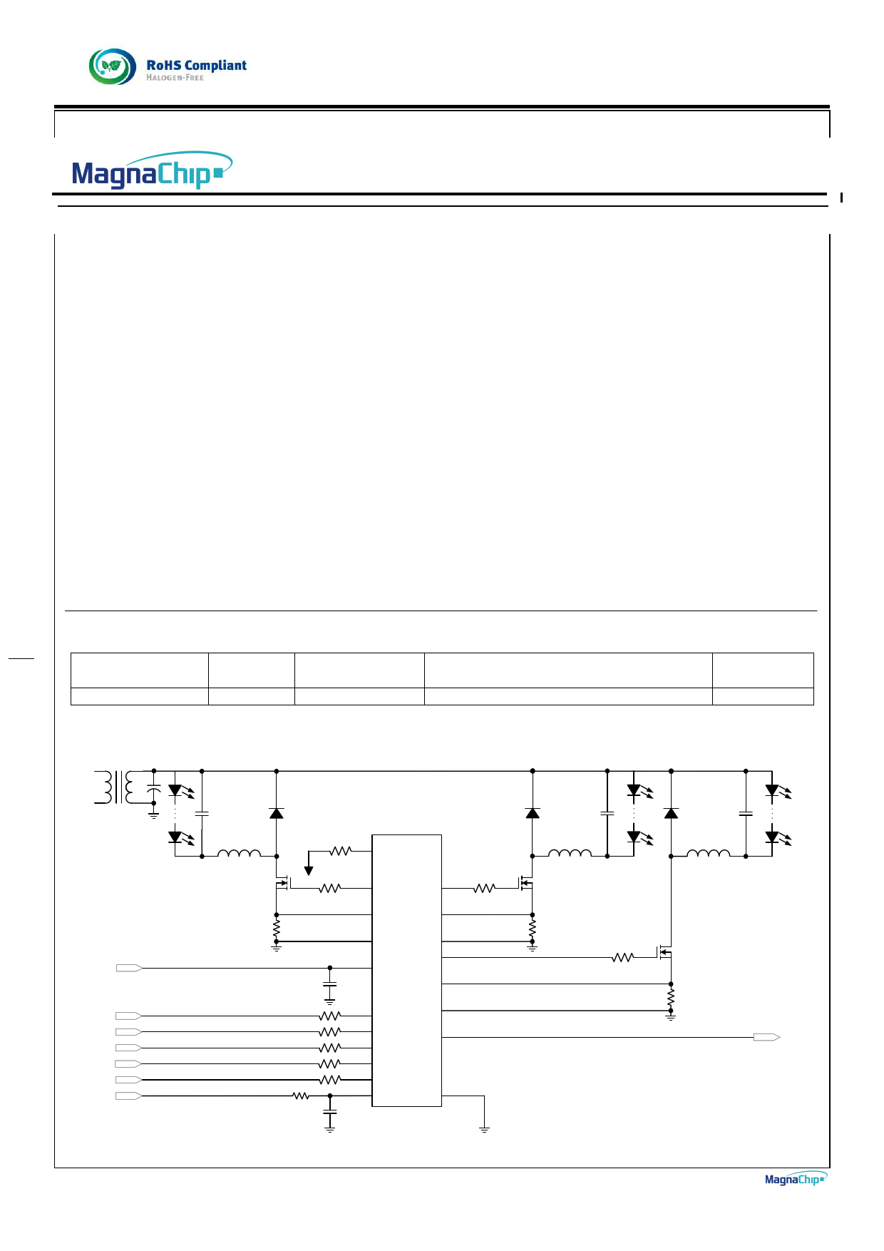
Typical Application
VCC
SEL
MODE
PWM1
PWM2
PWM3
ADIM
MAP3613
TOFF
GATE1 GATE2
CS1
CS2
PGND1
VCC
PGND2
GATE3
CS3
SEL
MODE
PWM1
PWM2
PWM3
ADIM
PGND3
FLT
GND
FLT
Mar 28th 2016
1 page 
Confidential
Electrical Characteristics
Unless noted, VVCC = 12V, CVCC = 1.0F, and typical values are tested at TA = 25C.
Parameter
Test Condition
Supply
VVCC Input Voltage Range
IQ Quiescent Current
VPWM = 5V, VCS = 0V
VUVLO
Under Voltage Lockout
Threshold Voltage on VCC pin
OFF Timer
Release threshold(rising VVCC)
Lockout hysteresis(falling VVCC)
tOFF GATEx Off-time
tON_MIN Min. On-Time (Note 1)
tON_MAX Max. On-Time
tOFF_MIN Min. Off-Time
DMAX Max. Duty Cycle (Note 1)
GATE Driver
RTOFF=52kΩ
RTOFF=104kΩ
VADIM = 3V
VADIM = 3V, tOFF=1.2us
ISOURCE GATEx Source Current
ISINK GATEx Sink Current
tRISE GATEx Output Rising Time
tFALL GATEx Output Falling Time
Current Sense & Dimming
VGATEx = 0V,
VGATEx = VVCC=12V
CGATEx=1nF, VVCC = 12V
CGATEx=1nF, VVCC = 12V
VADIM
AV
ADIM Input Voltage Range
VADIM to CSx Voltage Ratio
VCSx
CSx Voltage
tLEB Leading Edge Blanking Time
Logic Interface
VADIM = 0.5V
VADIM = 3.0V
(Note 1)
5
VPWMx
Logic Input Level on
PWMx pins
RPWMx Pull-down Resistor on PWMx pins
VMODE Logic Input Level on MODE pin
RMODE Pull-down Resistor on MODE pin
VSEL Logic Input Level on SEL pin
RSEL
Pull-down Resistor on SEL pin
Protection
VSCP
SCP Detection Threshold Voltage
on CS pins
VPWMx_L : Logic Low
VPWMx_H : Logic High
VPWMx = 4V
VMODE_L : Logic Low
VMODE_H : Logic High
VMODE = 4V
VSEL_L : Logic Low
VSEL_H : Logic High
VSEL = 4V
tDELAY
SCP Delay Time
tRESTART
VCSP
Restart Time
RCS Short Detection
Threshold Voltage on CS pin
tCSP RCS Short Detection Time
VSCPDS
MOSFET DS Short Detection
Threshold Voltage on CS pin
VPWMx_H : Logic High
VPWMx_L : Logic Low
tSCPDS
VOPEN
tOPEN
tOPENMASK
VFLT
RFLT
DOD1
DOD2
tOD
MOSFET DS Short Detection Time
Free-wheeling Diode Open
Detection Threshold Voltage on CS pin
Free-wheeling Diode Open Detection
Time
Free-wheeling Diode Open Detection
Mask Time
FLT pin High Voltage
FLT pin Internal Resistance
Protection Duty for OD1
Protection Duty for OD2
Auto-Restart time for OD1/2
fGATE=50kHz
(Note 1)
IFLT=100uA
VMODE = GND or Floating
Note 1: These parameters, although guaranteed by design, are not tested in mass production.
Mar 28th 2016
Datasheet Version 1.0
Min Typ Max Unit
8.5 18 V
5 mA
7.5 8.0 8.5
0.5 1.0 1.5
V
4.5 5.0 5.5
9 10 11
300
37
1.2 1.5
97
us
ns
us
us
%
400 mA
800 mA
50 85 ns
25 45 ns
0.5
0.2512
1.5073
0.5075
300
3.0
0.2563
1.5377
V
V/V
V
ns
0.8
V
2.0
50 100 150 kΩ
0.8
V
2.0
50 100 150 kΩ
0.8 V
2.0
50 100 150 kΩ
2.375
0.15
2.375
0.65
0.17
4.5
500
55
35
2.500
300
1
0.20
30
2.500
0.70
30
0.20
320
200
1000
57
37
200
2.625
0.25
2.625
0.75
0.23
5
1500
59
39
V
ns
ms
V
us
V
us
V
us
ns
V
Ω
%
%
ms
5 Page 
Confidential
Datasheet Version 1.0
Functional Description
GENERAL DESCRIPTION
TOFF SETTING
The MAP3613 is a 3-channel low-side single switch
control, constant off-time buck controller optimized to
LED backlight applications. The IC employs unique
average-mode current control architecture which
provides precise LED current accuracy. It does not
require any external loop compensation or high side
current sensing.
The IC operates at continuous conduction mode to
reduce output ripple, thus small output capacitor is
available. The off-time is user adjustable through the
selection of an external resistor, this allows the design
to be optimized for a given switching frequency range
and supports wide range of input voltages.
MAX. ON-TIME
The max. on-time of GATE is limited according to
ADIM voltage as following graph.
The off-time of the GATE driver is programmed by an
external resistor connected between the TOFF pin and
ground. Do not leave this pin open. The off-time is
calculated by following equation.
RTOFF
0.4 tOFF[us]1000[k]
38.4
LED CURRENT
The LED current is calculated by following equation.
I LED
0.5075 VADIM
RCS
[ A]
The ADIM voltage range is from 0.5V to 3V.
In terms of total system accuracy of LED current, the
larger inductance and the slower switching frequency,
the better accuracy.
PWM DIMMING
The brightness control of the LEDs is performed by a
11 pulse-width modulation. The GATE output is valid only
at PWM on period. This means that the GATE
maintains off-state as long as PWM signal is logic low.
Care should be taken to test at low PWM duty-cycle
because the output capacitor can affect rising and
falling time of LED current due to its charging and
discharging time.
SOFT-START
Care should be taken to choose input voltage which
should not exceed this on-time limit(especially OD2
mode).
The on-time of GATE can be calculated by following
equations.
D VLED
VIN
tOFF [us]
38.4
400
RTOFF
[k]
tON
D tOFF
1 D
Finally, tON < tON_MAX_Min Value
The MAP3613 operates at peak current mode at initial
start-up and every rising edge of PWM input to smooth
inductor current ramp-up(output capacitor charging
phase). The number of peak-controlled switch cycles is
8 times at initial start-up and 2 times at every PWM
rising edge as following figure.
UVLO_H
VCC
PWM
GATE
VCS
IL
VADIM*0.5075
8 times
2 times
Mar 28th 2016
11 Page | ||
| Páginas | Total 16 Páginas | |
| PDF Descargar | [ Datasheet MAP3613.PDF ] | |
Hoja de datos destacado
| Número de pieza | Descripción | Fabricantes |
| MAP3612 | 2-CH Average Current Control Buck Controller | MagnaChip |
| MAP3613 | 3-CH Average Current Control Buck Controller | MagnaChip |
| Número de pieza | Descripción | Fabricantes |
| SLA6805M | High Voltage 3 phase Motor Driver IC. |
Sanken |
| SDC1742 | 12- and 14-Bit Hybrid Synchro / Resolver-to-Digital Converters. |
Analog Devices |
|
DataSheet.es es una pagina web que funciona como un repositorio de manuales o hoja de datos de muchos de los productos más populares, |
| DataSheet.es | 2020 | Privacy Policy | Contacto | Buscar |