|
|
|
PDF ISL15100 Data sheet ( Hoja de datos )
| Número de pieza | ISL15100 | |
| Descripción | PLC Differential Line Driver | |
| Fabricantes | Intersil | |
| Logotipo | ||
Hay una vista previa y un enlace de descarga de ISL15100 (archivo pdf) en la parte inferior de esta página. Total 9 Páginas | ||
|
No Preview Available !
Single Port, PLC Differential Line Driver
ISL15100
The ISL15100 is a single port differential line driver developed
for Power Line Communication (PLC) applications. The device
is designed to drive heavy line loads while maintaining the
high level of linearity required in OFDM PLC modem links. With
15.5dBm of total transmit signal power into 100Ω line load,
the driver achieves -43dB average MTPR distortion across the
output spectrum up to 86MHz.
The ISL15100 has two bias current control pins (C0, C1) to
allow for four power settings (disable, low, medium, high). In
disable mode, the line driver outputs maintain a high
impedance in the presence of high receive signal amplitude,
so it doesn’t affect TDM receive signal integrity.
The ISL15100 is available in the thermally-enhanced 16 Ld
QFN and is specified for operation over the full -40°C to +85°C
ambient temperature range.
Features
• Single differential driver
• 100MHz Broadband PLC G.hn, EOC, HomePlug AV2
• Control pins for enable/disable and supply current selection
• High output impedance when disabled for TDM operation
• -43dBc average MTPR distortion at full line power
• Single +12V or bipolar ±6V nominal supplies
• High surge current handling capability
Applications
• Power Line Communication differential driver
• Pin compatible upgrade to ISL1571IRZ
Related Literature
• AN1325 “Choosing and Using Bypass Capacitors”
PART #
ISL1571
TABLE 1. ALTERNATE SOLUTIONS
NOMINAL ±VS
(V)
BANDWIDTH
(MHz)
APPLICATIONS
±6, +12
200 HomePlug AV1
100n
500
AFE
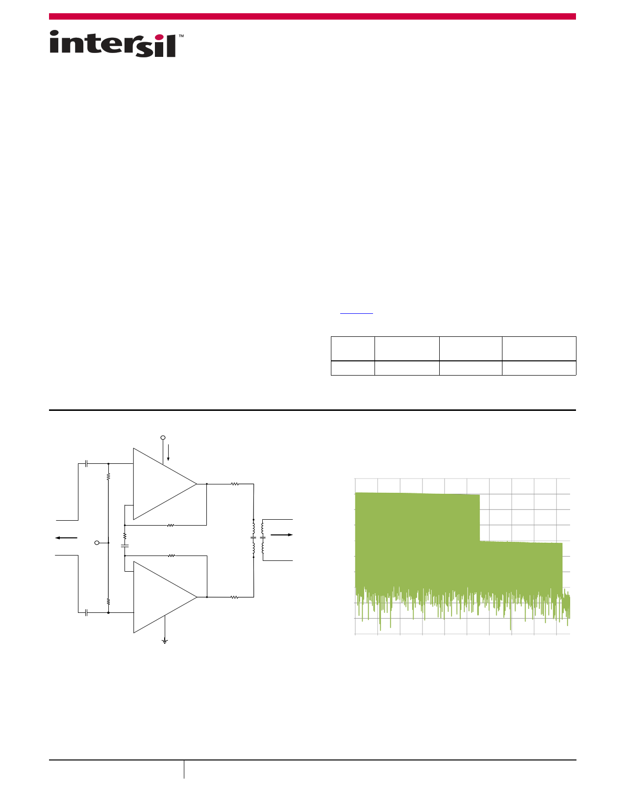
Rg
Vcm 133
2.2n
+12V
SUPPLY
DECOUPLING
+ NOT SHOWN
½ ISL15100
-
Rf
1kΩ
3.9
Rf
1kΩ
-
1:2
100Ω
NOMINAL
LINE
500
100n
½ ISL15100
+
3.9
TYPICAL DIFFERENTIAL I/O LINE DRIVER
FIGURE 1. TYPICAL APPLICATION CIRCUIT
-30
-40
-50
-60
-70
-80
-90
-100
-110
-120
-130
2
7 12 17 22 27 32 37 42 47
FREQUENCY (MHz)
FIGURE 2. 50MHz PLC SPECTRUM
September 19, 2013
FN8577.0
1
CAUTION: These devices are sensitive to electrostatic discharge; follow proper IC Handling Procedures.
1-888-INTERSIL or 1-888-468-3774 | Copyright Intersil Americas LLC 2013. All Rights Reserved
Intersil (and design) is a trademark owned by Intersil Corporation or one of its subsidiaries.
All other trademarks mentioned are the property of their respective owners.
1 page 
ISL15100
Electrical Specifications VS+ = +12V, VS- = GND = 0V, see Figure 3, Full Bias (C0 = C1 = 0V), TA = +25°C, unless otherwise specified.
PARAMETER
DESCRIPTION
CONDITIONS
MIN MAX
(Note 6) TYP (Note 6) UNIT
Inverting Input Bias Current Mismatch IB-DM
Difference between the INA- and INB- input -35 0 35 µA
bias currents
Inverting Input Bias Current Common
Mode
IB-CM
Average inverting input bias currents
(Note 7)
-90 -30 55 µA
Input Offset Voltage
VIOA, VIOB
Voltage difference from INA+ to INA- and
-85
0
85 mV
from INB+ to INB-
Input Offset Voltage Mismatch
Input Offset Voltage Common Mode
VIODM
VIOCM
VIOA - VIOB
Average offset voltage across the two
inputs
-5 0 5 mV
-80 20 80 mV
Differential Mode Output Offset Voltage VOSDM
Output referred total effect of all
differential DC error terms
-7.8 0 7.8 mV
Common Mode Output Offset Voltage VOSCM
Output referred total effect of all common -105 40 145 mV
mode DC errors
Input Headroom to Positive Supply
(VS+) - VIN(MAX)
INA+ and INB+ required margin to VS+
supply
3V
Input Headroom to Negative Supply
VIN(MIN) - (VS-)
INA+ and INB+ required margin to VS-
supply
3V
OUTPUT CHARACTERISTICS
Output Swing
VO-OPEN
VS = ±6V, Differential RLOAD ≥ 1kΩ, each
output pin voltage range
±4.85
±5.0
V
VO-LOADED
VS = ±6V, VO in linear region, Differential
RLOAD = 29Ω, each output pin voltage
range.
±4.6
V
VS = ±6V, VO driven into the rail, differential
RLOAD = 29Ω, each output pin voltage
range.
±4.2
±4.7
V
Output Current
POWER SUPPLY
IO
Linear output current (not short circuit)
±300 ±400
mA
Bipolar Supply Range
±VS
Symmetric supply, pin 4 at GND for logic
±4
±6 ±6.6
V
reference
Single Supply Range
VS+
Single supply with VS- and pin 4 at GND
8
Positive Supply Currents
IS+ (Full bias)
VO(DIFF) = 0V, C0 = C1 = 0V
27
IS+ (Medium bias) VO(DIFF) = 0V, C0 = 3.3V, C1 = 0V
19
IS+ (Low bias)
VO(DIFF) = 0V, C0 = 0V, C1 = 3.3V
12
IS+ (Power down) C0 = C1 = 3.3V
5.5
C0, C1 Input High Current
IINH, C0 or C1
C0 = C1 = 3.3V (Note 7)
-150
C0, C1 Input Low Current
IINL, C0 or C1
C0 = C1 = 0V (Note 7)
-1.5
C0, C1 Logic High Voltage
VINH
Pin 4 at GND, logic reference pin
2
C0, C1 Logic Low Voltage
VINL
Pin 4 at GND, logic reference pin
-0.3
NOTES:
6. Compliance to data sheet limits is assured by one or more methods: production test, characterization and/or design.
7. Positive currents flow out of the pin.
12
32
23
15
7
-90
1
3.3
0
13.2
37
26
18
8.5
-30
1.5
5.5
0.8
V
mA
mA
mA
mA
µA
µA
V
V
5 FN8577.0
September 19, 2013
5 Page | ||
| Páginas | Total 9 Páginas | |
| PDF Descargar | [ Datasheet ISL15100.PDF ] | |
Hoja de datos destacado
| Número de pieza | Descripción | Fabricantes |
| ISL15100 | PLC Differential Line Driver | Intersil |
| Número de pieza | Descripción | Fabricantes |
| SLA6805M | High Voltage 3 phase Motor Driver IC. |
Sanken |
| SDC1742 | 12- and 14-Bit Hybrid Synchro / Resolver-to-Digital Converters. |
Analog Devices |
|
DataSheet.es es una pagina web que funciona como un repositorio de manuales o hoja de datos de muchos de los productos más populares, |
| DataSheet.es | 2020 | Privacy Policy | Contacto | Buscar |