|
|
|
PDF ZXGD3005E6 Data sheet ( Hoja de datos )
| Número de pieza | ZXGD3005E6 | |
| Descripción | 25V 10A GATE DRIVER | |
| Fabricantes | Diodes | |
| Logotipo | ||
Hay una vista previa y un enlace de descarga de ZXGD3005E6 (archivo pdf) en la parte inferior de esta página. Total 8 Páginas | ||
|
No Preview Available !
A Product Line of
Diodes Incorporated
ZXGD3005E6
25V 10A GATE DRIVER IN SOT26
Description and Applications
The ZXGD3005E6 is a high-speed non-inverting single gate driver
capable of driving up to 10A into a MOSFET or IGBT gate capacitive
load from supply voltages up to 25V. With propagation delay times
down to <10ns and correspondingly rise/fall times of <20ns.
This gate driver ensures rapid switching of the MOSFET or IGBT to
minimize power losses and distortion in high current switching
applications. It is ideally suited to act as a voltage buffer between the
typically high output impedances of a controller IC and the effectively
low impedance on the gate of a power MOSFET or IGBT during
switching. Its low input voltage requirement and high current gain
allows high current driving from low voltage controller ICs.
The ZXGD3005E6 has separate source and sink outputs that enables
the turn-on and turn-off times of the MOSFET or IGBT to be
independently controlled. In addition, the wide supply voltage range
allows full enhancement of the MOSFET or IGBT to minimize on-state
losses and permits +15V to -5V gate drive voltage to prevent dV/dt
induced false triggering of IGBTs. The ZXGD3005E6 has been
designed to be inherently rugged to latch-up and shoot-through
issues. The optimized pin-out SOT26 package eases board layout,
enabling reduced parasitic inductance of traces.
Power MOSFET and IGBT Gate Driving in:
• Synchronous switch-mode power supplies
• Power Factor Correction (PFC) in power supplies
• Secondary side synchronous rectification
• Plasma Display Panel power modules
• 1, 2 and 3-phase motor control circuits
• Audio switching amplifier power output stages
• Solar inverters
Features and Benefits
• Emitter-follower configuration for ultra-fast switching
• <10ns propagation delay time
• <20ns rise/fall time
• Non-inverting voltage buffer stage
• Wide supply voltage up to 25V to minimize on-losses
• 10A peak current drive into capacitive loads
• Low input current of 1mA to deliver 4A output current
• Separate source and sink outputs for independent control of rise
and fall time
• Optimized pin-out to ease board layout and minimize parasitic
inductance of traces
• Rugged design that avoids latch-up or shoot-through issues
• Near - Zero quiescent supply current
• “Lead-Free”, RoHS Compliant (Note 1)
• “Green” Devices (Note 2)
• Qualified to AEC-Q101 Standards for High Reliability
Mechanical Data
• Case: SOT26
• Case material: Molded Plastic. “Green” Molding Compound.
• UL Flammability Rating 94V-0
• Moisture Sensitivity: Level 1 per J-STD-020
• Terminals: Matte Tin Finish
• Weight: 0.018 grams (approximate)
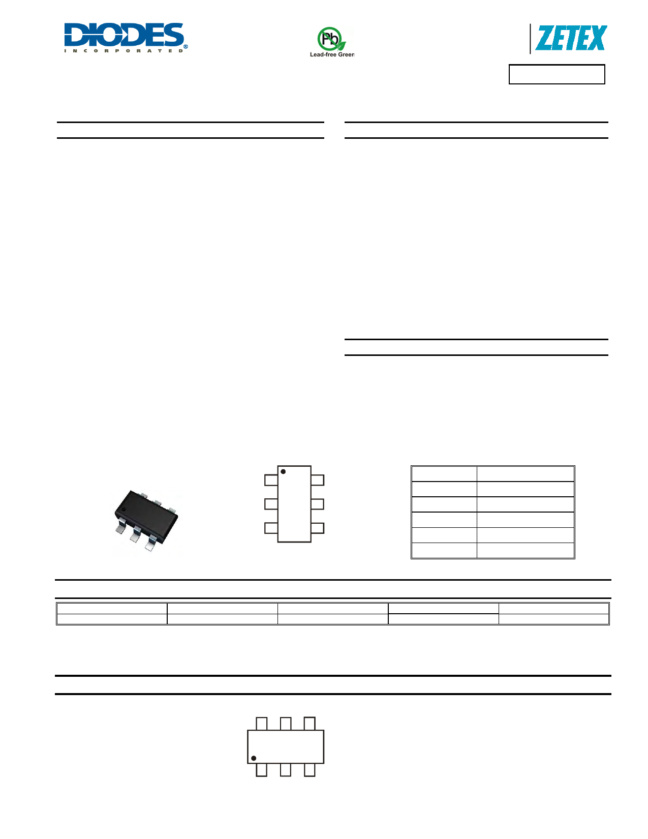
SOT26
1
Top View
VCC Source
IN Do Not Connect
VEE Sink
Top View
Pin-Out
Pin Name
VCC
IN
VEE
SOURCE
SINK
Pin Function
Supply voltage high
Driver input pin
Supply voltage low
Source current output
Sink current output
Ordering Information (Note 3)
Product
ZXGD3005E6TA
Marking
3005
Reel size (inches)
7
Tape width (mm)
8
Quantity per reel
3000
Notes:
1. No purposefully added lead
2. “Green” devices, Halogen and Antimony Free, Diodes Inc’s “Green” Policy can be found on our website at http://www.diodes.com
3. For packaging details, go to our website at http://www.diodes.com
Marking Information
3005
3005 = Product Type Marking Code
ZXGD3005E6
Document Number DS35095 Rev. 4 – 2
1 of 8
www.diodes.com
March 2011
© Diodes Incorporated
1 page 
A Product Line of
Diodes Incorporated
ZXGD3005E6
Typical Switching Characteristics @TA = 25°C unless otherwise specified
10 10
1
C =1uF
L
C =100nF
L
0.1
0.01
VIN = 15V
VCC= 15V
VEE= 0V
RL = 0.18Ω
C =10nF
L
C =1nF
L
1k 10k 100k 1M 10M
R Input Resistance (Ω)
IN
Source Current vs. Input Resistance
1
C =1uF
L
C =100nF
L
0.1
0.01
VIN = 15V
VCC= 15V
VEE= 0V
RL = 0.18Ω
C =10nF
L
C =1nF
L
1k 10k 100k 1M 10M
R Input Resistance (Ω)
IN
Sink Current vs. Input Resistance
1000
R =1MΩ
IN
R =100kΩ
IN
100
1000
R =1MΩ
IN
R =100kΩ
IN
100
10
1
1
R =200Ω
IN
R =1kΩ
IN
10
R =10kΩ
IN
100
VVIINN == 1155VV
VVCCCC== 1155VV
VVEEEE== 00VV
RRLL == 00..1188ΩΩ
1k
C Load Capacitance (nF)
L
Turn-On Delay Time
10
R =200Ω
IN
1
1
R =1kΩ
IN
10
R =10kΩ
IN
100
VIN = 15V
VCC= 15V
VEE= 0V
RL = 0.18Ω
1k
C Load Capacitance (nF)
L
Turn-Off Delay Time
10000
R =1MΩ
IN
R =100kΩ
1000 IN
10000
R =1MΩ
IN
1000
R =100kΩ
IN
100
R =10kΩ
IN
10
R =200Ω
IN
R =1kΩ
IN
VIN = 15V
VCC= 15V
VEE= 0V
RL = 0.18Ω
1 10 100
C Load Capacitance (nF)
L
Turn-On Rise Time
1k
100
R =10kΩ
IN
10
R =200Ω
IN
R =1kΩ
IN
VIN = 15V
VCC= 15V
VEE= 0V
RL = 0.18Ω
1 10 100 1k
C Load Capacitance (nF)
L
Turn-Off Fall Time
ZXGD3005E6
Document Number DS35095 Rev. 4 – 2
5 of 8
www.diodes.com
March 2011
© Diodes Incorporated
5 Page | ||
| Páginas | Total 8 Páginas | |
| PDF Descargar | [ Datasheet ZXGD3005E6.PDF ] | |
Hoja de datos destacado
| Número de pieza | Descripción | Fabricantes |
| ZXGD3005E6 | 25V 10A GATE DRIVER | Diodes |
| Número de pieza | Descripción | Fabricantes |
| SLA6805M | High Voltage 3 phase Motor Driver IC. |
Sanken |
| SDC1742 | 12- and 14-Bit Hybrid Synchro / Resolver-to-Digital Converters. |
Analog Devices |
|
DataSheet.es es una pagina web que funciona como un repositorio de manuales o hoja de datos de muchos de los productos más populares, |
| DataSheet.es | 2020 | Privacy Policy | Contacto | Buscar |