|
|
|
PDF ZSSC3224 Data sheet ( Hoja de datos )
| Número de pieza | ZSSC3224 | |
| Descripción | High End 24-Bit Sensor Signal Conditioner IC | |
| Fabricantes | IDT | |
| Logotipo | ||
Hay una vista previa y un enlace de descarga de ZSSC3224 (archivo pdf) en la parte inferior de esta página. Total 30 Páginas | ||
|
No Preview Available !
High End 24-Bit Sensor Signal
Conditioner IC
ZSSC3224
Datasheet
Brief Description
The ZSSC3224 is a sensor signal conditioner (SSC) IC
for high-accuracy amplification and analog-to-digital con-
version of a differential or pseudo-differential input
signal. Designed for high-resolution sensor module
applications, the ZSSC3224 can perform offset, span,
and 1st and 2nd order temperature compensation of the
measured signal. Developed for correction of resistive
bridge or absolute voltage sensors, it can also provide a
corrected temperature output measured with an internal
sensor.
The measured and corrected sensor values are provided
at the digital output pins, which can be configured as I2C
(≤ 3.4MHz) or SPI (≤ 20MHz). Digital compensation of
signal offset, sensitivity, temperature, and non-linearity is
accomplished via a 26-bit internal digital signal
processor (DSP) running a correction algorithm.
Calibration coefficients are stored on-chip in a highly
reliable, non-volatile, multiple-time programmable (MTP)
memory. Programming the ZSSC3224 is simple via the
serial interface. The interface is used for the PC-
controlled calibration procedure, which programs the set
of calibration coefficients in memory. The ZSSC3224
provides accelerated signal processing, increased
resolution, and improved noise immunity in order to
support high-speed control, safety, and real-time sensing
applications with the highest requirements for energy
efficiency.
Features
Flexible, programmable analog front-end design; up
to 24-bit analog-to-digital converter (ADC)
Fully programmable gain amplifier for optimizing
sensor signals: gain range 6.6 to 216 (linear)
Internal auto-compensated 18-bit temperature sensor
Digital compensation of individual sensor offset; 1st
and 2nd order digital compensation of sensor gain as
well as 1st and 2nd order temperature gain and offset
drift
Programmable interrupt operation
High-speed sensing: e.g., 18-bit conditioned sensor
signal measurement rate >200s-1
Typical sensor elements can achieve an accuracy of
better than ±0.10% FSO* at -40 to 85°C
Benefits
Integrated 26-bit calibration math digital signal
processor (DSP)
Fully corrected signal at digital output
Layout customized for die-die bonding with sensor for
high-density chip-on-board assembly
One-pass calibration minimizes calibration costs
No external trimming, filter, or buffering components
required
Highly integrated CMOS design
Integrated reprogrammable non-volatile memory
Excellent for low-voltage and low-power battery
applications
Optimized for operation in calibrated resistive
(e.g., pressure) sensor or calibrated absolute voltage
(e.g., thermopile) sensor modules
Physical Characteristics
Supply voltage range: 1.68V to 3.6V
Operating mode current: ~1.0mA (typical)
Sleep Mode current: 20nA (typical)
Temperature resolution: <0.7mK/LSB
Excellent energy-efficiency:
with 18-bit resolution: <100pJ/step
with 24-bit resolution: <150nJ/step
Operation temperature: –40°C to +85°C
Small die size
Delivery options: die for wafer bonding
* FSO = Full Scale Output.
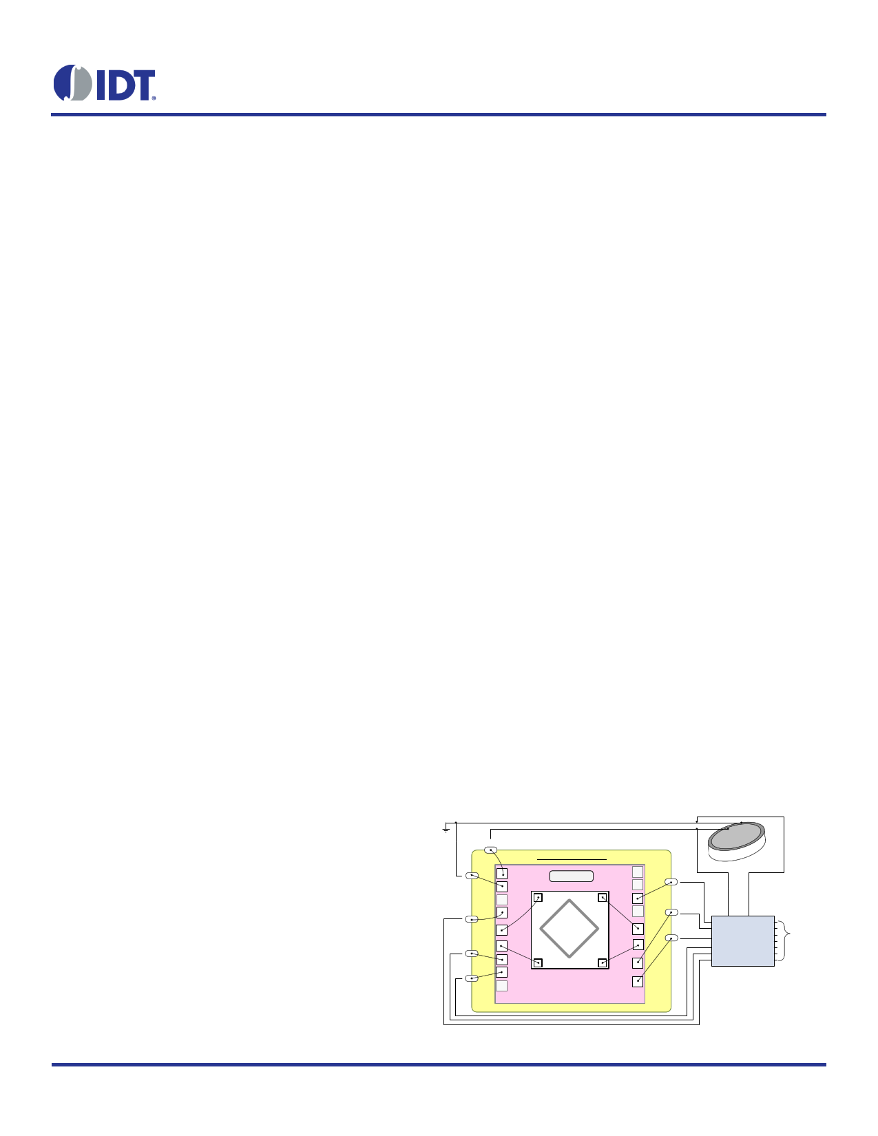
ZSSC3224 Application Example
VSS
RES
EOC
MISO
VDD
Stacked-Die Sensor Module
VDD
VSS
RES
ZSSC3224
VDDB
INP(+)
SS
VDDB
INN
EOC
MISO
sensor element
INN(-)
VSSB
INP
VSSB
MOSI
SDA
SCLK
SCL
VSS
VDD
Battery
SS
MOSI
SDA
SCLK
SCL
Microcontroller
© 2016 Integrated Device Technology, Inc
1
October 24, 2016
1 page 
ZSSC3224 Datasheet
List of Tables
Table 1.1
Table 1.2
Table 1.3
Table 1.4
Table 2.1
Table 2.2
Table 2.3
Table 2.4
Table 2.5
Table 2.6
Table 3.1
Table 3.2
Table 3.3
Table 3.4
Table 3.5
Table 3.6
Table 3.7
Table 3.8
Table 3.9
Table 4.1
Table 4.2
Table 4.3
Maximum Ratings.............................................................................................................................................................................6
Operating Conditions........................................................................................................................................................................6
Requirements for VDD Power-on Reset...........................................................................................................................................7
Electrical Parameters .......................................................................................................................................................................7
Amplifier Gain: Stage 1...................................................................................................................................................................12
Amplifier Gain: Stage 2...................................................................................................................................................................12
Gain Polarity ...................................................................................................................................................................................12
ADC Conversion Times for a Single Analog-to-Digital Conversion ................................................................................................13
ADC Offset Shift .............................................................................................................................................................................14
Typical Conversion Times versus Noise Performance with Full Sensor Signal Conditioning for Measurement including AZSM,
SM, AZTM, and TM (Bridge-Type Sensor).....................................................................................................................................15
SPI/I2C Commands ........................................................................................................................................................................24
Get_Raw Commands .....................................................................................................................................................................26
General Status Byte .......................................................................................................................................................................27
Mode Status ...................................................................................................................................................................................27
MTP Memory Content Assignments...............................................................................................................................................32
Measurement Results of ADC Raw Measurement Request (Two’s Complement) ........................................................................45
Calibration Coefficients (Factors and Summands) in Memory (Sign Magnitude) ...........................................................................45
Output Results from SSC-Correction Math or DSP—Sensor and Temperature ............................................................................45
Interrupt Thresholds TRSH1 and TRSH2—Format as for SSC-Correction Math Output ...............................................................45
Pad Assignments............................................................................................................................................................................46
Physical Package Dimensions .......................................................................................................................................................48
Pin Assignments PQFN24..............................................................................................................................................................48
© 2016 Integrated Device Technology, Inc
5
October 24, 2016
5 Page 
ZSSC3224 Datasheet
Figure 2.2 ZSSC3224 Functional Block Diagram with Voltage-Source Sensor
VDDB
VTP Temperature
Reference
VTN Sensor
AGND / CM
Generator
Vreg int
Bias Current
Generator
Voltage
Regulator
Power Ctr.
ZSSC3224
VDD
VSS
INP
INN
VSSB
Pre-
Amplifier
Power-On
Reset (POR)
Clock
Generator
Oscillator
A
D
24-Bit
System
Control
Unit
DSP Core
(Calculations,
Communication)
EOC
MTP
SPI
I²CTM
SCLK/SCL
SS
MOSI/SDA
MISO
RES
The amplifier consists of two stages with programmable gain values.
The ZSSC3224 employs a programmable analog-to-digital converter (ADC) optimized for conversion speed and noise
suppression. The programmable resolution from 12 to 24 bits provides flexibility for adapting the conversion
characteristics. To improve power supply noise suppression, the ADC uses the bridge supply VDDB as its reference
voltage leading to a ratiometric measurement topology if the external sensor is a bridge-type element.
The remaining ZSSC3224-internal offset and the sensor element offset, i.e., the overall system offset for the amplifier and
ADC, can be canceled by means of an offset and auto-zero measurement, respectively.
The DSP accomplishes the auto-zero, span, and 1st and 2nd order temperature compensation of the measured external
sensor signal. The correction coefficients are stored in the MTP memory.
The ZSSC3224 supports SPI and I2C interface communication for controlling the ZSSC3224, configuration, and
measurement result output.
2.3. Analog Front End
2.3.1. Amplifier
The amplifier has a fully differential architecture and consists of two stages. The amplification of each stage and the
external sensor gain polarity are programmable via settings in the Measurement Configuration Register SM_config1 and
SM_config2 (addresses 12HEX and 16HEX; see section 3.6.2) in the MTP memory (for details, see section 2.4.2).
Note: Only one of these two possible configurations is used for the measurement. The default configuration is
SM_config1. Alternately, SM_config2 can be implemented by sending a command to select this configuration for the
measurement (see section 3.5.1). The term SM_config is used in explanations for general register content and
functionality for both SM_config1 and SM_config2, as the registers’ bit assignments are exactly the same for both
registers.
The first 6 bits of SM_config are the programmable gain settings Gain_stage1 and Gain_stage2. The options for the
programmable gain settings are listed in Table 2.1 and Table 2.2.
© 2016 Integrated Device Technology, Inc
11
October 24, 2016
11 Page | ||
| Páginas | Total 30 Páginas | |
| PDF Descargar | [ Datasheet ZSSC3224.PDF ] | |
Hoja de datos destacado
| Número de pieza | Descripción | Fabricantes |
| ZSSC3224 | High End 24-Bit Sensor Signal Conditioner IC | IDT |
| Número de pieza | Descripción | Fabricantes |
| SLA6805M | High Voltage 3 phase Motor Driver IC. |
Sanken |
| SDC1742 | 12- and 14-Bit Hybrid Synchro / Resolver-to-Digital Converters. |
Analog Devices |
|
DataSheet.es es una pagina web que funciona como un repositorio de manuales o hoja de datos de muchos de los productos más populares, |
| DataSheet.es | 2020 | Privacy Policy | Contacto | Buscar |