|
|
|
PDF ADP1052 Data sheet ( Hoja de datos )
| Número de pieza | ADP1052 | |
| Descripción | Digital Controller for Isolated Power Supply | |
| Fabricantes | Analog Devices | |
| Logotipo | ||
Hay una vista previa y un enlace de descarga de ADP1052 (archivo pdf) en la parte inferior de esta página. Total 30 Páginas | ||
|
No Preview Available !
Data Sheet
Digital Controller for Isolated
Power Supply with PMBus Interface
ADP1052
FEATURES
GENERAL DESCRIPTION
Peak data telemetry recording
The ADP1052 is an advanced digital controller with a PMBus™
High speed input voltage feedforward control
interface targeting high density, high efficiency, dc-to-dc power
6 pulse-width modulation (PWM) logic outputs with 625 ps
conversion. This controller implements voltage mode control with
resolution
high speed, input line feedforward for enhanced transient and
Switching frequency: 49 kHz to 625 kHz
improved noise performance. The ADP1052 has six programmable
Frequency synchronization as master and slave device
pulse-width modulation (PWM) outputs capable of controlling
Multiple energy saving modes
most high efficiency power supply topologies, with added control
Adaptive dead time compensation for efficiency optimization
of synchronous rectification (SR). The device includes adaptive
Low power consumption: 100 mW typical
dead time compensation to improve efficiency over the load range,
Direct parallel control for power supplies without OR’ing devices
and programmable light load mode operation, combined with
Accurate droop current share
low power consumption, to reduce system standby power losses.
Prebias startup
Reverse current protection
Conditional overvoltage protection
Extensive fault detection and protection
PMBus compliant
Graphical user interface (GUI) for ease of programming
On-board EEPROM for programming and data storage
Available in a 24-lead, 4 mm × 4 mm LFCSP
The ADP1052 implements several features to enable a robust
system of parallel and redundant operation for customers that
require high availability or parallel connection. The device provides
synchronization, reverse current protection, prebias startup,
accurate current sharing between power supplies, and conditional
overvoltage techniques to identify and safely shut down an
erroneous power supply in parallel operation mode.
−40°C to +125°C operating temperature
The ADP1052 is based on flexible state machine architecture
APPLICATIONS
and is programmed using an intuitive GUI. The easy to use
interface reduces design cycle time and results in a robust,
High density isolated dc-to-dc power supplies
hardware coded system loaded into the built-in EEPROM. The
Intermediate bus converters
small size (4 mm × 4 mm) LFCSP package makes the ADP1052
High availability parallel power systems
ideal for ultracompact, isolated dc-to-dc power module or
Server, storage, industrial, networking, and communications
embedded power designs.
infrastructure
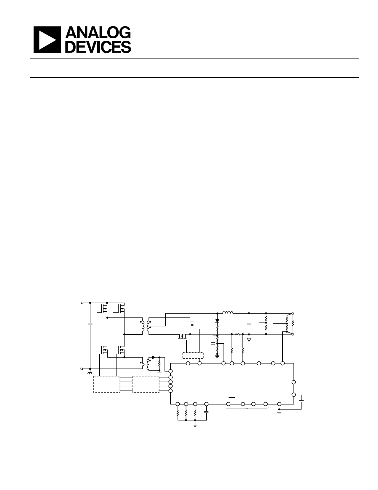
TYPICAL APPLICATIONS CIRCUIT
DC
INPUT
LOAD
DRIVER
iCoupler®
DRIVER
SR1 SR2
CS1
OUTA
OUTB
OUTC
OUTD
RES ADD RTD VCORE
VF CS2– CS2+ OVP VS+ VS–
ADP1052
SYNI/FLGI
VDD
PG/ALT CTRL SDA SCL AGND
PMBus
Figure 1.
Rev. A
Document Feedback
Information furnished by Analog Devices is believed to be accurate and reliable. However, no
responsibilityisassumedbyAnalogDevices for itsuse,nor foranyinfringementsofpatentsor other
rights of third parties that may result from its use. Specifications subject to change without notice. No
license is granted by implication or otherwise under any patent or patent rights of Analog Devices.
Trademarksandregisteredtrademarksarethepropertyoftheirrespectiveowners.
One Technology Way, P.O. Box 9106, Norwood, MA 02062-9106, U.S.A.
Tel: 781.329.4700
©2015 Analog Devices, Inc. All rights reserved.
Technical Support
www.analog.com
1 page 
ADP1052
Data Sheet
SPECIFICATIONS
VDD = 3.0 V to 3.6 V, TJ = −40°C to +125°C, unless otherwise noted; FSR = full-scale range.
Table 1.
Parameter
SUPPLY
Supply Voltage
Supply Current
POWER-ON RESET
Power-On Reset
UVLO Threshold
UVLO Hysteresis
Overvoltage Lockout (OVLO) Threshold
OVLO Debounce
VCORE PIN
Output Voltage
OSCILLATOR AND PLL
PLL Frequency
Digital PWM Resolution
OUTA, OUTB, OUTC, OUTD, SR1, SR2 PINS
Output Voltage
Low
High
Rise Time
Fall Time
Output Current
Source
Sink
Synchronization Signal Output (SYNO)
Positive Pulse Width
VS+, VS− VOLTAGE SENSE PINS
Input Voltage Range
Leakage Current
Voltage Sense (VS) Accurate Analog-to-
Digital Converter (ADC)
Valid Input Voltage Range
ADC Clock Frequency
Register Update Rate
Measurement
Resolution
Accuracy
Temperature Coefficient
Voltage Differential from VS− to AGND
Symbol Min
VDD 3.0
IDD
UVLO
OVLO
2.75
3.7
VCORE
2.45
190
Typ Max Unit
3.3
33
IDD + 6
50
3.6
100
V
mA
mA
μA
3.0 V
2.85 2.97 V
35 mV
3.9 4.1 V
2 μs
500 μs
2.6 2.75 V
200 210 MHz
625 ps
Test Conditions/Comments
2.2 μF capacitor connected to AGND
Normal operation; PWM pins unloaded
During EEPROM programming
Shutdown; VDD below undervoltage
lockout (UVLO)
VDD rising
VDD falling
VDD_OV flag debounce set to 2 μs
VDD_OV flag debounce set to 500 μs
330 nF capacitor connected to AGND
RES input = 10 kΩ (±0.1%)
VOL 0.4 V
VOH VDD − 0.4
V
tR 3.5 ns
tF 1.5 ns
IOH = 10 mA
IOL = −10 mA
CLOAD = 50 pF
CLOAD = 50 pF
IOL −10
mA
IOH 10 mA
600 640 680 ns OUTC or OUTD programmed as SYNO
VIN 0
1 1.6 V Differential voltage from VS+ to VS−
1.0 μA
0
−5
−80
−2
−32
−1.0
−16
−200
1.6 V
1.56 MHz
10 ms
12 Bits
Factory trimmed at 1.0 V
+5 % FSR 0% to 100% of input voltage range
+80 mV
+2 % FSR 10% to 90% of input voltage range
+32 mV
+1.0 % FSR 900 mV to 1.1 V
+16 mV
70 ppm/°C
+200 mV
Rev. A | Page 4 of 113
5 Page 
ADP1052
PIN CONFIGURATION AND FUNCTION DESCRIPTIONS
Data Sheet
VS– 1
VS+ 2
CS2– 3
CS2+ 4
VF 5
CS1 6
ADP1052
TOP VIEW
18 VCORE
17 PG/ALT
16 CTRL
15 SDA
14 SCL
13 SYNI/FLGI
NOTES
1. FOR INCREASED RELIABILITY OF THE SOLDER
JOINTS AND MAXIMUM THERMAL CAPABILITY,
IT IS RECOMMENDED THAT THE EXPOSED PAD
BE SOLDERED TO THE PCB AGND PLANE.
Figure 3. Pin Configuration
Table 4. Pin Function Descriptions
Pin No. Mnemonic Description
1 VS−
Inverting Voltage Sense Input. This pin is the connection for the ground line of the power rail. Provide a low
ohmic connection to AGND. To allow for trimming, it is recommended that the resistor divider on this input have
a tolerance specification of ≤0.5%.
2 VS+
Noninverting Voltage Sense Input. This pin signal is referred to VS−. To allow for trimming, it is recommended
that the resistor divider on this input have a tolerance specification of ≤0.5%.
3 CS2−
Inverting Differential Current Sense Input. For best operation, use a nominal voltage of 1.12 V with this pin. When
using low-side current sensing, place a 4.99 kΩ level shifting resistor between the sense resistor and this pin.
When using high-side current sensing in a 12 V application, place a 5.62 kΩ resistor between the sense resistor
and this pin. When using high-side current sensing, apply the formula R = (VOUT − 1.12 V)/1.915 mA. A 0.1%
resistor must be used to connect this circuit. If this pin is not used, connect it to AGND and set the CS2 current
sense to high-side current sense mode (Register 0xFE19[7] = 1 binary).
4 CS2+
Noninverting Differential Current Sense Input. For best operation, use a nominal voltage of 1.12 V with this pin.
When using low-side current sensing, place a 4.99 kΩ level shifting resistor between the sense resistor and this
pin. When using high-side current sensing in a 12 V application, place a 5.62 kΩ resistor between the sense
resistor and this pin. When using high-side current sensing, apply the formula R = (VOUT − 1.12 V)/1.915 mA.
A 0.1% resistor must be used to connect this circuit. If this pin is not used, connect it to AGND and set the CS2
current sense to high-side current sense mode (Register 0xFE19[7] = 1 binary).
5 VF
Feedforward/Voltage Sense/UVLO Protection. Three optional functions can be implemented with this pin:
feedforward, primary side input voltage sensing, and input voltage UVLO protection. This pin is connected
upstream of the output inductor through a resistor divider network. The nominal voltage at this pin should be
1 V. This signal is referred to AGND.
6 CS1
Primary Side Current Sense Input. This pin is connected to the primary side current sensing ADC and to the cycle-
by-cycle current-limit comparator. This signal is referred to AGND. The resistors on this input must have a
tolerance specification of ≤0.5% to allow for trimming. When not in use, connect this pin to AGND.
7 SR1
PWM Logic Output Drive. This signal is referred to AGND. When not in use, disable this pin.
8 SR2
PWM Logic Output Drive. This signal is referred to AGND. When not in use, disable this pin.
9 OUTA PWM Logic Output Drive. This signal is referred to AGND. When not in use, disable this pin.
10 OUTB
PWM Logic Output Drive. This signal is referred to AGND. When not in use, disable this pin.
11 OUTC
PWM Logic Output Drive. This signal is referred to AGND. This pin can also be programmed as a synchronization
signal output (SYNO). When not in use, disable this pin.
12 OUTD
PWM Logic Output Drive. This signal is referred to AGND. This pin can also be programmed as a synchronization
signal output (SYNO). When not in use, disable this pin.
13 SYNI/FLGI Synchronization Signal Input/External Signal Input to Generate a Flag Condition. When not in use, connect this
pin to AGND.
14 SCL
I2C/PMBus Serial Clock Input and Output (Open-Drain). This signal is referred to AGND.
15 SDA
I2C/PMBus Serial Data Input and Output (Open-Drain). This signal is referred to AGND.
16 CTRL
PMBus Control Signal. It is recommended that a 1 nF capacitor be connected from the CTRL pin to AGND for
noise debounce and decoupling. This signal is referred to AGND.
Rev. A | Page 10 of 113
11 Page | ||
| Páginas | Total 30 Páginas | |
| PDF Descargar | [ Datasheet ADP1052.PDF ] | |
Hoja de datos destacado
| Número de pieza | Descripción | Fabricantes |
| ADP1050 | Digital Controller | Analog Devices |
| ADP1051 | Digital Controller | Analog Devices |
| ADP1052 | Digital Controller for Isolated Power Supply | Analog Devices |
| ADP1053 | 3-Channel Digital Power Supply Controller | Analog Devices |
| Número de pieza | Descripción | Fabricantes |
| SLA6805M | High Voltage 3 phase Motor Driver IC. |
Sanken |
| SDC1742 | 12- and 14-Bit Hybrid Synchro / Resolver-to-Digital Converters. |
Analog Devices |
|
DataSheet.es es una pagina web que funciona como un repositorio de manuales o hoja de datos de muchos de los productos más populares, |
| DataSheet.es | 2020 | Privacy Policy | Contacto | Buscar |