|
|
PDF UPD8257-5 Data sheet ( Hoja de datos )
| Número de pieza | UPD8257-5 | |
| Descripción | PROGRAMMABLE DMA CONTROLLER | |
| Fabricantes | NEC | |
| Logotipo |  |
|
Hay una vista previa y un enlace de descarga de UPD8257-5 (archivo pdf) en la parte inferior de esta página. Total 8 Páginas | ||
|
No Preview Available !
NEe Microcomputers, Inc.
NEe
JLPD8257
JLPD8257·5
PROGRAMMABLE DMA CONTROLLER
DESCR IPTION
The !1PD8257-5 is a programmable four-channel Direct Memory Access (DMA) con-
troller. It is designed to simplify high speed transfers between peripheral devices and
memories. Upon a peripheral request, the !1PD8257-5 generates a sequential memory
address, thus allowing the peripheral to read or write data directly to or from memory.
Peripheral requests are prioritized within the !1PD8257-5 so that the system bus may
be acquired by the generation of a single HOLD command to the 8080A. DMA cycle
counts are maintained for each of the four channels, and a control signal notifies the
peripheral when the preprogrammed member of DMA cycles has occurred. Output con-
trol signals are also provided which allow simplified sectored data transfers and expan-
sion to other !1PD8257-5 devices for systems requiring more than four DMA channels.
FEATU RES • NEC Now Supplies !1PD8257-5 to !1PD8257 Requirements
• Four Channel DMA Controller
• Priority DMA Request Logic
• Channel Inhibit Logic
• Terminal Count and Modulo 128 Outputs
• Automatic Load Mode
• Single TTL Clock
• Single +5V Supply ± 10%
• Expandable
• 40 Pin Plastic Dual-In-Line Package
PIN CONFIGURATION
MEMR
MARK
READY
HlDA
ADDSTB
AEN
HRQ
Cs
ClK
RESET
DACK2
DACK3
DRQ3
oRQ2
DRQ1
DRQO
GND
IlPD
8257/
8257-5
A7
A6
AS
A4
TC
A3
A2
A,
AO
vcc
DO
D,
D2
D3
~
DACKO
DACK,
Os
06
07
0]"00
A]"AO
IIOR
IIOW
MEMR
MEMW
ClK
RESET
READY
HRO
HlDA
AEN
ADSTB
TC
MARK
DRQ3·0RDo
DACK3·DACKO
CS
vCC
GND
PIN NAMES
Data Bus
Address Bus
tID Read
1/0 Write
Memory Read
Memory Write
Clock Input
Reset Input
Ready
Hold Request (to SOSOA)
Hold Acknowledge (from 8080A)
Address Enable
Address Strobe
Terminal Count
Modulo 128 Mark
DMA Request Input
DMA Acknowledge Out
Chip Select
+5 Volts
Ground
REV/3
617
1 page 
JLPD8257-5
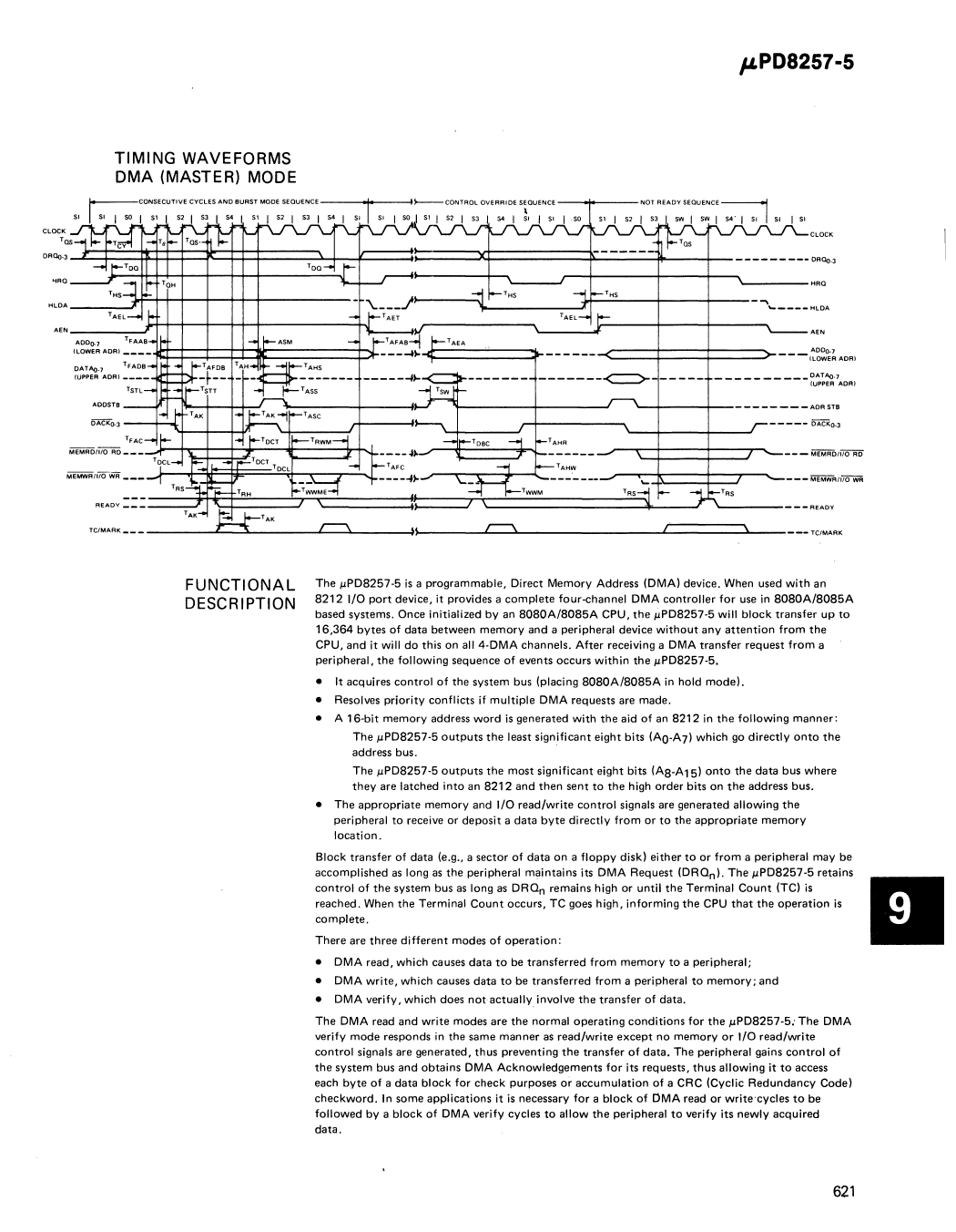
TIMING WAVEFORMS
DMA (MASTER) MODE
DRao.3....JC*~=I:Fj:::j:=1:=*=R=I===::;Lk-4c==~~====xj:=======*:.:.====Il-~.::::..-4-----------DAOO.3
1~---~~-=~--~-1~~~-_1---t_----~'-----HLDA
-<===:1====1:===:::>---- (~~~ ADR)
-------<::::>-
__________ DATAo-7
(UPPER ADRl
"--+---t--------- - ADR STS
- - - - - i5ACKO•3
~,....,;:::j::==::j:==7. . . .--- - M'EMRo/ilOFiO
=TCfMARK ______ =TA< __..J~t::::::::j;:......=. __'c__\C:::)~___.U. :;.....---...J.c--\=:::..-------___,c.'=====L__
FUNCTIONAL
DESCRIPTION
The /LPDS257-5 is a programmable, Direct Memory Address (DMA) device. When used with an
S212 I/O port device, it provides a complete four-channel DMA controller for use in SOSOA/SOS5A
based systems. Once initialized by an SOSOA/SOS5A CPU, the ILPDS257-5 will block transfer up to
16,364 bytes of data between memory and a peripheral device without any attention from the
CPU, and it will do this on all 4-DMA channels. After receiving a DMA transfer request from a
peripheral, the following sequence of events occurs within the /LPDB257-5.
• It acquires control of the system bus (placing SOSOA/BOB5A in hold mode).
• Resolves priority conflicts if multiple DMA requests are made.
• A 16-bit memory address word is generated with the aid of an 8212 in the following manner:
The /LPDS257-5 outputs the least significant eight bits (AO-A7) which go directly onto the
address bus.
.
The /LPDS257-5 outputs the most significant eight bits (AB-A15) onto the data bus where
they are latched into an B212 and then sent to the high order bits on the address bus.
• The appropriate memory and I/O read/write control signals are generated allowing the
peripheral to receive or deposit a data byte directly from or to the appropriate memory
location.
Block transfer of data (e.g., a sector of data on a floppy disk) either to or from a peripheral may be
accomplished as long as the peripheral maintains its DMA Request (DROn ). The /LPDS257-5 retains
control of the system bus as long as DROn remains high or until the Terminal Count (TC) is
reached. When the Terminal Count occurs, TC goes high, informing the CPU that the operation is
complete.
There are three different modes of operation:
• DMA read, which causes data to be transferred from memory to a peripheral;
• DMA write, which causes data to be transferred from a peripheral to memory; and
• DMA verify, which does nOl"actually involve the transfer of data.
The DMA read and write modes are the normal operating conditions for the /LPDS257-5: The DMA
verify mode responds in the same manner as read/write except no memory or I/O read/write
control signals are generated, thus preventing the transfer of data. The peripheral gains control of
the system bus and obtains DMA Acknowledgements for its requests, thus allowing it to access
each byte of a data block for check purposes or accumulation of a CRC (Cyclic Redundancy Code)
checkword. In some applications it is necessary for a block of OMA read or write'cycles to be
followed by a block of DMA verify cycles to allow the peripheral to verify its newly acquired
data.
II
621
5 Page | ||
| Páginas | Total 8 Páginas | |
| PDF Descargar | [ Datasheet UPD8257-5.PDF ] | |
Hoja de datos destacado
| Número de pieza | Descripción | Fabricantes |
| UPD8257-5 | PROGRAMMABLE DMA CONTROLLER | NEC |
| Número de pieza | Descripción | Fabricantes |
| SLA6805M | High Voltage 3 phase Motor Driver IC. |
Sanken |
| SDC1742 | 12- and 14-Bit Hybrid Synchro / Resolver-to-Digital Converters. |
Analog Devices |
|
DataSheet.es es una pagina web que funciona como un repositorio de manuales o hoja de datos de muchos de los productos más populares, |
| DataSheet.es | 2020 | Privacy Policy | Contacto | Buscar |
