|
|
PDF CDP1883 Data sheet ( Hoja de datos )
| Número de pieza | CDP1883 | |
| Descripción | CMOS 7-Bit Latch and Decoder Memory Interfaces | |
| Fabricantes | GE | |
| Logotipo |  |
|
Hay una vista previa y un enlace de descarga de CDP1883 (archivo pdf) en la parte inferior de esta página. Total 5 Páginas | ||
|
No Preview Available !
CMOS Perlpherals,_ _ _ _ _ _ _ _ _ _ _ _ _ _ _ _ _ _ _ _ _ _ _ _ _ __
CDP1883, CDP1883C
CLOCK
01'0
20 VDD
I. A8
""...2
18 A.
17 AID
...."'3
01"
I,.. '"
"2
..A. m
"13 CST
IT
VSS
10
12 CS2
" en
TOP VIEW
92CS-37283
CDP1883, CDP1883C
TERMINAL ASSIGNMENT
CMOS 7-Bit Latch and Decoder
Memory Interfaces
Features:
• Performs memory address latch and decoder functions multiplexed or
non-multiplexed
• Interfaces directly with the CDP1800-series microprocessors
• Allows decoding for systems up to 32K bytes
The RCA-CDP1883 IS a CMOS 7-blt memory latch and
decoder Circuit Intended for use In CDP1800-series micro-
processor systems It can serve as a direct Interface
between the multiplexed address bus of thiS system and up
to four 8K x 8-blt memories to Implement a 32K-byte
memory system With four 4K x 8-blt memOries, a 16K-byte
system can be decoded
Thedevice is also compatible with non-multiplexed address
bus microprocessors By connecting the clock inputto Vee,
the latches are In the data-following mode and the decoded
outputs can be used In general-purpose memory-system
applications
The CDP1833 IS compatible with CDP1800-series micro-
processors operating at maximum clock frequency.
The CDP1883 and CDP1883C are functionally identical.
They differ in that the CDP1883 has a recommended
operallng voltage range of 4 to 10.5 volts and the C version
has a recommended operating voltage range of 4 to 6.5
volts
The CDP1883 and CDP1883C are supplied in 20-lead, dual-
in-line plastiC packages (E suffix).
MAXIMUM RATINGS, Absolute-Maximum Values:
DC SUPPLY-VOLTAGE RANGE, (VDD)
(Voltage referenced to VSS terminal)
CDP1883........... .. .........................................................................................-05to+11 V
CDP1883C ....................................................................................................-05to+7V
INPUT VOLTAGE RANGE, ALL INPUTS. . ................................................................... -0 5 to VDD +05 V
DC INPUT CURRENT, ANY ONE INPUT ................................................................................ ±10 mA
POWER DISSIPATION PER PACKAGE (PO)
For TA;-40 to +60·C (PACKAGE TYPE E) .. ............................. .. ........................................ 500 mW
For TA;+60 to +85·C (PACKAGE TYPE E) .... ....... . .......... . ..................... Derate Linearly at 12 mW/·C to 200 mW
DEVICE DISSIPATION PER OUTPUT TRANSISTOR
For TA;FULL PACKAGE-TEMPERATURE RANGE ...................................................................... 100 mW
OPERATING-TEMPERATURE RANGE (TA)
PACKAGE TYPE E ................................................................................................ -40 to +85·C
STORAGE-TEMPERATURE RANGE (Tstg) .......................................................................... -65 to +150·C
LEAD TEMPERATURE (DURING SOLDERING)
At distance 1/16 ± 1/32 In (159 ± 0 79 mm) from case for 10 s max ..................................................... +265·C
File Number 1507
474 ______________________________________________________________
1 page 
CMOS Perlpherals,_ _ _ _ _ _ _ _ _ _ _ _ _ _ _ _ _ _ _ _ _ _ _ _......_
CDP1883, CDP1883C
APPLICATION INFORMATION
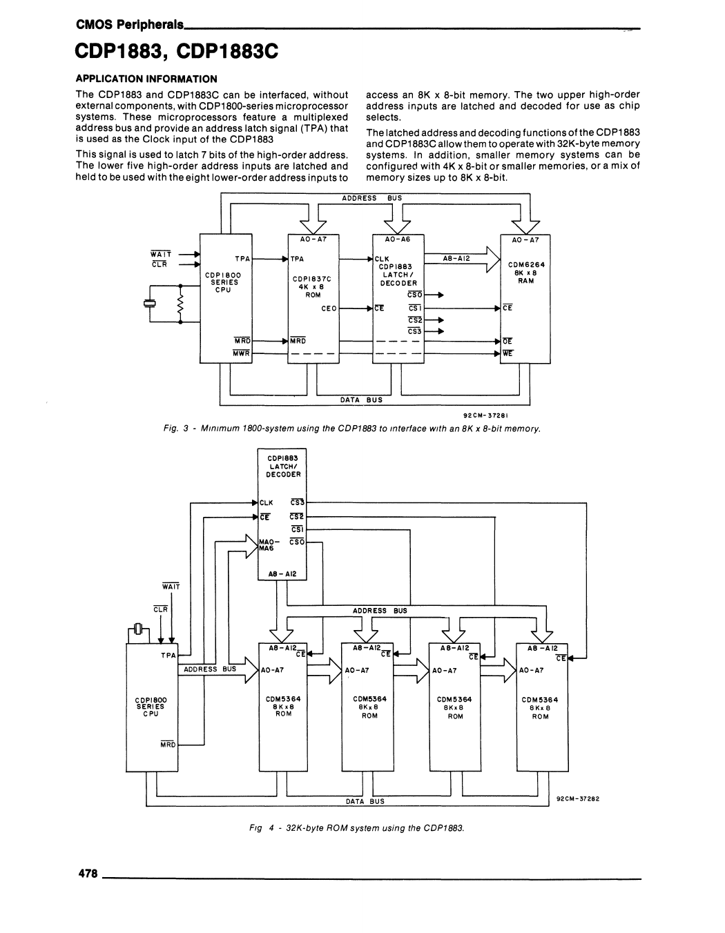
The CDP1883 and CDP1883C can be interfaced, without
external components, with CDP1800-series microprocessor
systems. These microprocessors feature a multiplexed
address bus and provide an address latch signal (TPA) that
is used as the Clock input of the CDP1883
This signal is used to latch 7 bits of the high-order address.
The lower five high-order address inputs are latched and
held to be used with the eight lower-order address inputs to
access an 8K x 8-bit memory. The two upper high-order
address inputs are latched and decoded for use as chip
selects.
The latched address and decoding functions of the CDP1883
and CDP1883C allow them to operate with 32K-byte memory
systems. In addition, smaller memory systems can be
configured with 4K x 8-bit or smaller memories, or a mix of
memory sizes up to 8K x 8-bit.
WATT
m
COP 1800
SERIES
CPU
CDPI837C
4K II. 8
ROM
'iiRli iiRo
Mii1f
CLK
COPI883
LATCH I
DECODER
m
CSi
rn
ill
----
A8-A12
CE
llr
WE"
92CM- 37281
Fig. 3 - Mmlmum 1800-system using the CDPl883 to mterface WIth an 8K x 8-bit memory.
CDPI883
LATCHI
DECODER
.-------~CLK
,..----"Irr
~r_--------------------------------------__;
ml---------------,
~~-------------
CSO
TPA
ADDRESS BUS
CDPIBOO
BERI ES
CPU
CDM5364
SKx8
ROM
COM53&4
SKxS
ROM
CDM5364
SKxS
ROM
CDM5364
SKitS
ROM
FIg 4 - 32K-byte ROM system using the CDP1883.
92CM-37282
478 ___________________________________________________________
5 Page | ||
| Páginas | Total 5 Páginas | |
| PDF Descargar | [ Datasheet CDP1883.PDF ] | |
Hoja de datos destacado
| Número de pieza | Descripción | Fabricantes |
| CDP1881 | CMOS 6-Bit Latch and Decoder Memory Interfaces | GE |
| CDP1881C | CMOS 6-Bit Latch and Decoder Memory Interfaces | Intersil Corporation |
| CDP1881C | CMOS 6-Bit Latch and Decoder Memory Interfaces | GE |
| CDP1882 | CMOS 6-Bit Latch and Decoder Memory Interfaces | Intersil Corporation |
| Número de pieza | Descripción | Fabricantes |
| SLA6805M | High Voltage 3 phase Motor Driver IC. |
Sanken |
| SDC1742 | 12- and 14-Bit Hybrid Synchro / Resolver-to-Digital Converters. |
Analog Devices |
|
DataSheet.es es una pagina web que funciona como un repositorio de manuales o hoja de datos de muchos de los productos más populares, |
| DataSheet.es | 2020 | Privacy Policy | Contacto | Buscar |
