|
|
|
PDF P2003ND5G Data sheet ( Hoja de datos )
| Número de pieza | P2003ND5G | |
| Descripción | N- & P-Channel Field Effect Transistor | |
| Fabricantes | NIKO-SEM | |
| Logotipo | ||
Hay una vista previa y un enlace de descarga de P2003ND5G (archivo pdf) en la parte inferior de esta página. Total 8 Páginas | ||
|
No Preview Available !
NIKO-SEM
N- & P-Channel Enhancement Mode
Field Effect Transistor
P2003ND5G
TO-252-5
Halogen-Free & Lead-Free
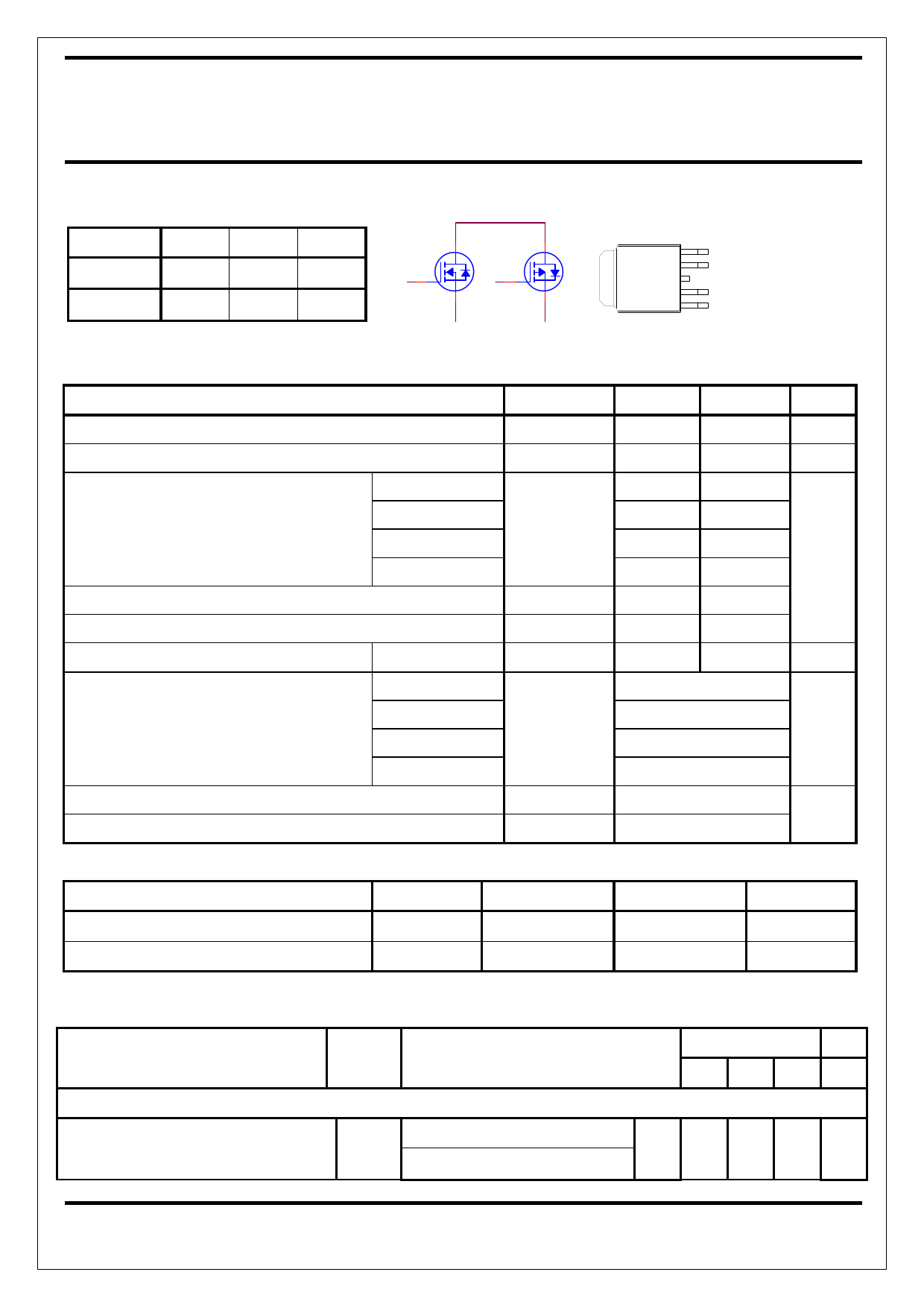
PRODUCT SUMMARY
V(BR)DSS RDS(ON)
N-Channel 30 20mΩ
P-Channel -30 36mΩ
ID
25A
-19A
D1
G1
S1
D2
G2
S2
G : GATE
D : DRAIN
S : SOURCE
ABSOLUTE MAXIMUM RATINGS (TC = 25 °C Unless Otherwise Noted)
PARAMETERS/TEST CONDITIONS
SYMBOL
Drain-Source Voltage
Gate-Source Voltage
Continuous Drain Current
Pulsed Drain Current2
TC = 25 °C
TC = 70 °C
TA = 25 °C
TA = 70 °C
Avalanche Current
Avalanche Energy
L = 0.1mH
TC = 25 °C
Power Dissipation
TC = 70 °C
TA = 25 °C
TA = 70 °C
Junction & Storage Temperature Range
Lead Temperature (1/16” from case for 10 sec.)
VDS
VGS
ID
IDM
IAS
EAS
PD
Tj, Tstg
TL
N-Channel P-Channel UNITS
30 -30 V
±20 ±20 V
25 -19
20 -15
9 -7
A
7 -5.7
65 -45
19 -18
18 17 mJ
21
13
W
3
2
-55 to 150
275
°C
THERMAL RESISTANCE RATINGS
THERMAL RESISTANCE
SYMBOL
TYPICAL
Junction-to-Case
RθJC
Junction-to-Ambient
RθJA
1 Pulse width limited by maximum junction temperature.
ELECTRICAL CHARACTERISTICS (TC = 25 °C, Unless Otherwise Noted)
PARAMETER
SYMBOL
TEST CONDITIONS
Drain-Source Breakdown Voltage
V(BR)DSS
STATIC
VGS = 0V, ID = 250μA
VGS = 0V, ID = -250μA
MAXIMUM
6
42
UNITS
°C / W
°C / W
LIMITS
UNIT
MIN TYP MAX
N-Ch 30
P-Ch -30
V
REV 1.0
May-21-2009
1
1 page 
NIKO-SEM
N- & P-Channel Enhancement Mode
Field Effect Transistor
P2003ND5G
TO-252-5
Halogen-Free & Lead-Free
Gate charge Characteristics
10
8
ID=6A
VDS=15V
6
4
2
0
02468
Qg , Total Gate Charge
10
Source-Drain Diode Forward Voltage
1 .0 E + 0 3
1 .0 E + 0 2
1 .0 E + 0 1
TJ =150°C
1 .0 E + 0 0
1 .0 E -0 1
TJ =25°C
1 .0 E -0 2
1 .0 E -0 3
1 .0 E -0 4
0.0
0.2 0.4
0.6 0.8 1.0
VSD, Source-To-Drain Voltage(V)
1.2
Safe Operating Area
100
Operation in This Are a
is Lim ited by RDS(ON)
↓
10
1
NOTE :
1.VGS= 10V
2.TC=25° C
3.RθJC = 6° C/W
4.Single Pulse
0.1
0.1 VDS, Drain1-To-Source Volta1g0 e(V)
100us
1ms
10m s
100m s
1S
10S
DC
100
Single Pulse Maximum Power Dissipation
500
450
400
350
SINGLE PULSE
RθJC = 6° C/W
TC=25° C
300
250
200
150
100
50
0
0.0001
0.001
0.01
0.1
Single Pulse Time(s)
1
10
1.00E+01
Transient Thermal Response Curve
1.00E+00
1.00E-01
1.00E-02
Duty Cycle=0.5
0.2
0.1
0.05
0.02
0.01
1.00E-03
single Pluse
1.00E-04
1.E-06
1.E-05
Note
1. Duty cycle, D= t1 / t2
2. RthJC = 6 ℃/W
43..TRJ-TthCJC=(Pt)*R=thJrC(t)*RthJC
1.E-04
1.E-03
1.E-02
1.E-01
T1 , Square Wave Pulse Duration[sec]
1.E+00
1.E+01
1.E+02
REV 1.0
May-21-2009
5
5 Page | ||
| Páginas | Total 8 Páginas | |
| PDF Descargar | [ Datasheet P2003ND5G.PDF ] | |
Hoja de datos destacado
| Número de pieza | Descripción | Fabricantes |
| P2003ND5G | N- & P-Channel Field Effect Transistor | NIKO-SEM |
| Número de pieza | Descripción | Fabricantes |
| SLA6805M | High Voltage 3 phase Motor Driver IC. |
Sanken |
| SDC1742 | 12- and 14-Bit Hybrid Synchro / Resolver-to-Digital Converters. |
Analog Devices |
|
DataSheet.es es una pagina web que funciona como un repositorio de manuales o hoja de datos de muchos de los productos más populares, |
| DataSheet.es | 2020 | Privacy Policy | Contacto | Buscar |