|
|
|
PDF TC57256D-20 Data sheet ( Hoja de datos )
| Número de pieza | TC57256D-20 | |
| Descripción | CMOS UV ERASABLE AND ELECTRICALLY PROGRAMMABEL READ ONLY MEMORY | |
| Fabricantes | Toshiba | |
| Logotipo | ||
Hay una vista previa y un enlace de descarga de TC57256D-20 (archivo pdf) en la parte inferior de esta página. Total 8 Páginas | ||
|
No Preview Available !
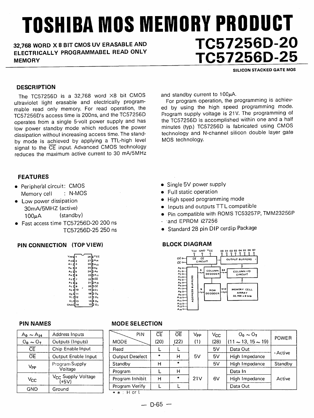
TOSHIBA MOS MEMORY PRODUCT
32,768 WORD X 8 BIT CMOS UV ERASABLE AND
ELECTRICALLY PROGRAMMABEL READ ONLY
MEMORY
TC57256D-20
TC57256D-25
SILICON STACKED GATE MOS
DESCRIPTION
The TC57256D is a 32,768 word X8 bit CMOS
ultraviolet light erasable and electrically program-
mable read only memory. For read operation, the
TC57256D's access time is 200ns, and the TC57256D
operates from a single 5-volt power supply and has
low power standby mode which reduces the power
dissipation without increasing access time. The stand-
by mode is achieved by applying a TTL-high level
signal to the CE input. Advanced CMOS technology
reduces the maximum active current to 30 mA/5MHz
and standby current to 100pA.
For program operation, the programming is achiev-
ed by using the high speed programming mode.
Program supply voltage is 21 V. The programming of
the TC57256D is accomplished within one and a half
minutes (typ.) TC57256D is fabricated using CMOS
technology and N-channel silicon double layer gate
MOS technology.
FEATURES
• Peripheral circuit: CMOS
Memory cell
N-MOS
• Low power dissipation
30mA/5MHZ (active)
100llA
(standby)
• Fast access time TC572560-20 200 ns
TC572560-25 250 ns
PIN CONNECTION (TOP VIEW)
• Single 5V power supply
• Full static operation
• High speed programming mode
• Inputs and outputs TTL compatible
• Pin compatible with ROMS TC53257P, TMM23256P
- 'and EPROM i27256
• Standard 28 pin DIP cerdip Package
BLOCK DIAGRAM
PIN NAMES
Ao ,...,A14
0 0 "", 0 7
CE
OE
Vpp
Vee
GND
Address Inputs
Outputs (Inputs)
Chip Enable Input
Output Enable Input
P~ograrn Supply
Voltage
Vee Supply Voltage
(+5V)
Ground
MODE SELECTION
~MODE
CE OE vpp vee
0 0 ,...,07
POWER
(20) (22) (1) (28) (11,..., 13,15,..., 19)
Read
Output Deselect
L
*
L 5V Data Out
• Active
H 5V 5V High Impedance
Standby
H*
5V High Impedance Standby
Program
LH
Data In
Program Inhibit H
*
21V
6V High Impedance
Active
Program Verify
* * , H or L
L
L
Data Out
0-65 -
1 page 
TC57256D-20
TC57256D-25
ERASURE CHARACTERISTICS
The TC57256D's erasure is achieved by applying
shortwave ultraviolet light which has a wavelength of
2537A (Angstroms) through the chips transparent
window.
The integrated dose (ultraviolet light intensity
[w/cm2] X exposure time [sec.]) for erasure should be
a minimum of 15 [w· sec/cm2]
When the Toshiba GL-15 sterilizing lamp is used
and the device is exposed at a distance of 1cm from
the lamp surface, the erasure will be achieved within
60 minutes.
And using commercial lamps with an ultraviolet light
intensity of 12000 [p.w/cm2] will reduce the exposure
time to about 20 minutes. (In this case, the integrated
dose is 12000 [p.w/cm2] X (20X60) [sec] ~ 15
[w· sec/cm2] .)
The TC57256D's erasure begins to occur when
exposed to light with wavelength shorter than 4000A.
Both sunlight and flourescent lamps include
3000-4000A wavelength components. Therefore
when used under such lighting for extended periods
of time, opaque seals-Toshiba EPROM Protect Seal
AC901-are available
OPERATION INFORMATION
The TC57256D's six operation modes are listed
in the following table. Mode selection can be achieved
by applying TTL level signal to all inputs.
r -M-O.D_E - - - - - -
Read Operation
(Ta';' -40 _ 85°(:)
Program Operation
(Ta = 25 ±5°C)
Read
Output Deselect
Standby
Program
Program1nhibit
Program Verify
CE OE Vpp vee
0 0 -07
(20) (22) (1) (28) (11-13,15-19)
LL
Data Out
* H 5V 5V High Impedance
H*
High Impedance
LH
Data In
H * 21V 6V High Impedance
LL
Data Out
POWER
Active
Active
Standby
Active
Active
Active
READ MODE
The TC57256D has two control functions. The chip
enable (CE) controls the operation power and should
be used for device selection.
The output enable (OE) controls the output buffers,
independent of device selection.
Assuming that CE=OE=VIL, the output data is valid
at the outputs after the address access _time from
stabilizing of all addressess.
The CE to output valid (tCE) time is equal to the
address access time (tACC).
Assuming that CE=VIL and all addresses are valid,
the output data is valid at the outputs after tOE from
the falling edge of CEo
- 0-69 -
5 Page | ||
| Páginas | Total 8 Páginas | |
| PDF Descargar | [ Datasheet TC57256D-20.PDF ] | |
Hoja de datos destacado
| Número de pieza | Descripción | Fabricantes |
| TC57256D-20 | CMOS UV ERASABLE AND ELECTRICALLY PROGRAMMABEL READ ONLY MEMORY | Toshiba |
| TC57256D-25 | CMOS UV ERASABLE AND ELECTRICALLY PROGRAMMABEL READ ONLY MEMORY | Toshiba |
| Número de pieza | Descripción | Fabricantes |
| SLA6805M | High Voltage 3 phase Motor Driver IC. |
Sanken |
| SDC1742 | 12- and 14-Bit Hybrid Synchro / Resolver-to-Digital Converters. |
Analog Devices |
|
DataSheet.es es una pagina web que funciona como un repositorio de manuales o hoja de datos de muchos de los productos más populares, |
| DataSheet.es | 2020 | Privacy Policy | Contacto | Buscar |