|
|
|
PDF TA8227P Data sheet ( Hoja de datos )
| Número de pieza | TA8227P | |
| Descripción | LOW FREQUENCY POWER AMPLIFIER | |
| Fabricantes | SUM | |
| Logotipo | ||
 1. - Toshiba ( PDF ) Hay una vista previa y un enlace de descarga de TA8227P (archivo pdf) en la parte inferior de esta página. Total 8 Páginas | ||
|
No Preview Available !
SUM
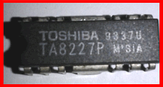
TA8227P
LOW FREQUENCY POWER AMPLIFIER TA8227P
GENERAL DESCRIPTION
TA8227P is audio power IC with built-in
two Channels developed for portable radio
cassette tape recorder with power ON/OFF
switch. Thermal shut down protection
circuit is built in. Because of the parts
reduction and DIP (Dual in line package),
space merit is remarkable.
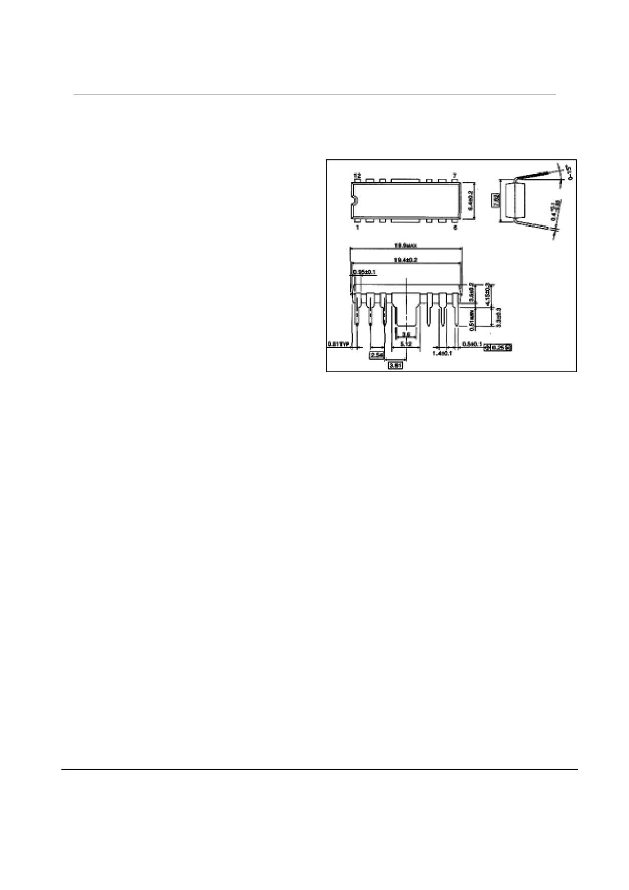
Outline Drawing TA
TA8227P
SUM****
F E AT U R E S
z High Power
Pout=2.5W/CH(Typ.) :(Vcc=9V,RL=4 Ω,f=1kHz,THD=10%)
Pout=3.0W/CH(Typ.) :(Vcc=9V,RL=3 Ω,f=1kHz,THD=10%)
z Vo ltage Gain : Gv=45dB(Typ.) Rf=120 ,f=1kHz
Gv=56.5dB(Typ.) Rf=0 ,f=1kHz
z Low popping noise at power ON
z Small Quiescent Current : ICCQ=21mA(Typ.) (Vcc=9V Vin=0)
z Ripple Rejection Ratio : R.R.=-52dB(Typ.)(Vcc=9V fripple=100Hz Rg=600
z Cross Talk : C.T.= -50dB(Typ.)(Vcc=9V f=1kHz Rg=600 )
z Output Noise Voltage : Vno=0.3mVrms(Typ.)(Vcc=9V
Rg=10k
BW=20Hz~20kHz)
z Stand-By Switch
z Soft Clip
z Built-in thermal shut down protection circuit
z Best for supply voltage 9V
z supply voltage range : Vcc=5~12V
)
SUM
1/8
1 page 
SUM
TA8227P
As the oscillation allowance varies according to the printed pattern layout, the
standard printed board is recommended to be referred to design it
5. INPUT VOLTAGE
When the excessive signal is input, turning-up is produced in the clip waveform.
Th e tu rn ing-u p po in t is VI N= 3 00 mVr ms ( Typ . ) : V c c =9 V, RL= 4 Ω, f=1k Hz : Enough care
must be taken for this phenomenon.
6. POWER ON/OFF SWITCH
There is power ON/OFF switch at pin 1. However, output power is changed by pin 1
supply voltage when pin 1 voltage in not same pin 12 supply voltage, after referring
to attached date, select pin 1 supply voltage.
7. GND LINE
GND pin is not separated for Pre-GND and for Pw-GND. That is liable to cause
distortion and cross talk worse. Before use this IC, please check it.
CHARACTERISTIC CURVES
SUM
5/8
5 Page | ||
| Páginas | Total 8 Páginas | |
| PDF Descargar | [ Datasheet TA8227P.PDF ] | |
Hoja de datos destacado
| Número de pieza | Descripción | Fabricantes |
| TA8227AP | LOW FREQUENCY POWER AMPLIFIER | Unisonic Technologies |
| TA8227P | LOW FREQUENCY POWER AMPLIFIER | SUM |
| TA8227P | LOW FREQUENCY POWER AMPLIFIER | Toshiba |
| TA8227P | LOW FREQUENCY POWER AMPLIFIER | Unisonic Technologies |
| Número de pieza | Descripción | Fabricantes |
| SLA6805M | High Voltage 3 phase Motor Driver IC. |
Sanken |
| SDC1742 | 12- and 14-Bit Hybrid Synchro / Resolver-to-Digital Converters. |
Analog Devices |
|
DataSheet.es es una pagina web que funciona como un repositorio de manuales o hoja de datos de muchos de los productos más populares, |
| DataSheet.es | 2020 | Privacy Policy | Contacto | Buscar |