|
|
|
PDF ZWIR4512 Data sheet ( Hoja de datos )
| Número de pieza | ZWIR4512 | |
| Descripción | Secure Low-Power Wireless IPv6 Module | |
| Fabricantes | IDT | |
| Logotipo | ||
Hay una vista previa y un enlace de descarga de ZWIR4512 (archivo pdf) en la parte inferior de esta página. Total 27 Páginas | ||
|
No Preview Available !
Secure Low-Power
Wireless IPv6 Module
ZWIR4512
Datasheet
Brief Description
The ZWIR4512 enables secure low-power wireless
IPv6 communication for sensors and small devices.
IDT provides a user-programmable, royalty-free
6LoWPAN stack with mesh routing capability with
the ZWIR4512. 6LoWPAN is an Internet Engineer-
ing Task Force (IETF) standard for building wireless,
low-power IP-based sensor and device networks.
These networks can easily be integrated into exist-
ing IT infrastructure or operate autonomously.
Secure communication is provided by standard-
compliant implementations of the Internet Protocol
Security (IPSec) protocol suite and the Internet Key
Exchange Protocol version 2 (IKEv2), which enable
highly secure end-to-end communication, including
over unsecure network nodes.
The module is powered by an ARM® Cortex™-M3
(ARM, Ltd. trademark) microcontroller and provides
a rich set of GPIO and peripheral interfaces. Up to
192kB of flash and 32kB of RAM are available for
applications. Different low power modes are pro-
vided to save energy in battery-operated devices.
The modules provide superior radio properties with-
out the need for complicated external RF design.
Benefits
• Uniquely simple programmability
• Standard-compliant security solution
• No need for external microcontroller
• Plug-and-play integration into local and wide-
area networks
• No RF design required
• 2D barcode label containing MAC address
• Superior radio propagation
• ETSI/FCC certified
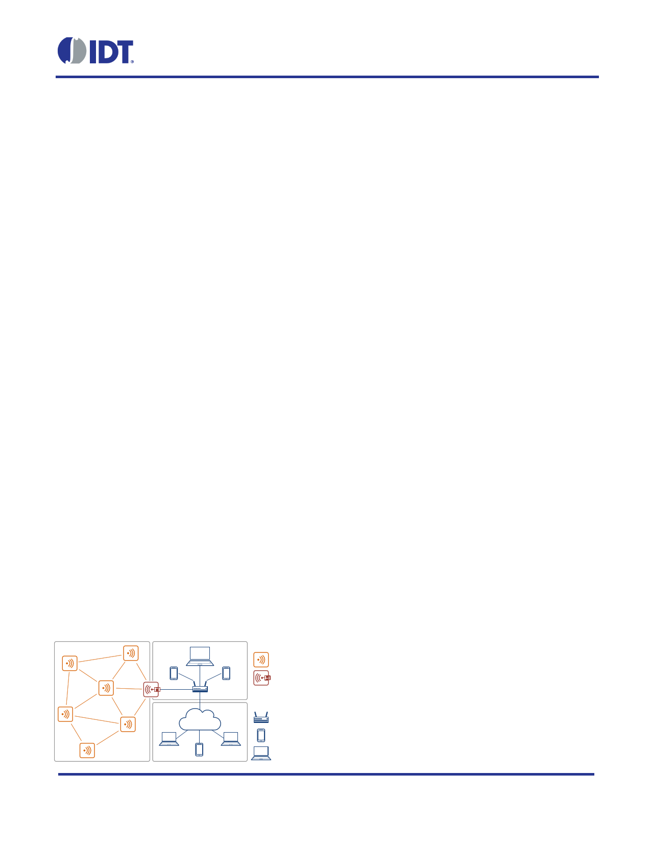
Typical ZWIR4512 Application Setup
LAN
Cloud /
Internet
PAN WAN
Specific Devices:
ZWIR45xx
Device
ZWIR45xx
Gateway
Off-the-Shelf
Components:
LAN
Router
Handheld
Device
Computer
Hardware Features
• License-free 868/915 MHz frequency bands
• ARM® Cortex™-M3 32-bit microcontroller
• ≤192kB flash and 32kB RAM for user applications
• Unique EUI64 address
• 4 channels in EU mode; 10 channels in US mode
• 19 (ZWIR4512AC1) or 21 (ZWIR4512AC2)
GPIOs with multiplexed peripheral functions:
2 x UART, SPI, 3 x ADC, 2 x DAC, 11 x PWM,
USB, CAN, I2C™ (NXP trademark), 8 x timer
Several 5V tolerant I/Os available
• Low current consumption: 3.5 µA in Standby
Mode; 10.5 mA in Receive Mode; 16.0 mA in
Transmit Mode @ 0 dBm
• Modulation schemes
BPSK (20 kBps EU, 40 kBps US)
O-QPSK (100 kBps EU, 250 kBps US)
• Receiver sensitivity: up to -110 dBm
• TX output power: up to 10 dBm (US Mode)
Firmware Features
• Serial command interface with built-in security
and over-the-air update (OTAU) functionality
• Royalty-free library bundle for custom firmware:
6LoWPAN communication library with mesh
routing capability; IPSec and IKEv2 security
libraries; over-the-air update library; several
peripheral libraries
Available Support
• Development Kit
• Programming guide and application notes
• Ethernet, USB and UART gateways
• Free packet sniffer and example programs
demonstrating C-API usage
• Windows® (Microsoft Corp. trademark) and
Linux® (Linus Torvalds trademark) support tools
Physical Characteristics
• Supply voltage: 2.0 V to 3.6 V
• Operating temperature: -40 °C to +85 °C
• 30-pin edge-board contact package or
32-pin land grid array package
© 2016 Integrated Device Technology, Inc.
1
January 27, 2016
1 page 
ZWIR4512 Datasheet
1 Module Characteristics
1.1. Absolute Maximum Ratings
The absolute maximum ratings are stress ratings only. The device might not function or be operable above the
operating conditions. Stresses exceeding the absolute maximum ratings might also damage the device. In
addition, extended exposure to stresses above the operating conditions might affect device reliability. IDT does
not recommend designing to the “Absolute Maximum Ratings.”
1.1.1. Voltage Characteristics
Parameter
Symbol
Min
Max
Unit
Main supply voltage
Backup supply voltage
Input voltage at 5V-tolerant GPIO pin
Input voltage at any other GPIO pin
VCC
VBAT
VGPIO
-0.3 4
-0.3 4
-0.3 5.5
-0.3 VCC+0.3
V
1.1.2. Current Characteristics
Parameter
Maximum total current consumption
Driving strength of each GPIOx pin
Driving strength of RF-control pins (PACTLN, PACTLP, DIG1)
Symbol
IVCC
IGPIO
IRFCTRL
Max
175
±25
8
Unit
mA
1.1.3. Thermal Characteristics
Parameter
Storage temperature range
Ambient temperature range
Symbol
TSTOR
TAMB
Value
-40 to +125
-40 to +85
Unit
°C
1.2. Operating Conditions
1.2.1. General Operating Conditions
Note: See important notes at the end of the table.
Parameter
Main supply voltage – ADC not used
Main supply voltage – ADC used
Backup supply voltage
Digital I/O high level input voltage
Digital I/O low level input voltage
Symbol
Min
Electrical Characteristics
VCC 2.0
VCC 2.4
VBKUP
1.8
VIH VCC – 0.4
VIL
Typ
Max
3.6
3.6
3.6
0.4
Unit
V
© 2016 Integrated Device Technology, Inc.
5
January 27, 2016
5 Page 
ZWIR4512 Datasheet
3 Application Circuits
ZWIR4512 modules are designed to require minimal external circuitry. The following sections illustrate how
modules must be connected in order to ensure proper power supply, reset behavior, programmability, and radio
performance. Instructions for the connection of GPIO pins are not given.
3.1. Power Supply
All internal components of the ZWIR4512 that require a stable power supply are internally decoupled with a
number of capacitors. Nevertheless, the module requires one external decoupling capacitor between VCC and
GND. This is the minimal external circuitry required for proper operation.
The module provides two different power supply pins: VCC and VSTDBY. VCC is the normal supply voltage that
must be applied in Run, Sleep, or Stop Mode. During Standby Mode, the module is powered by VSTDBY and VCC
can be switched off.
Figure 3.1 shows two possible power supply schemes. Scheme a) connects VSTDBY to the same voltage source
as VCC. This is the commonly used configuration. However, scheme b) allows switching off VCC in Standby
Mode. This can help reduce power dissipation in applications with ultra-low power requirements. During the
complete standby phase, VSTDBY is powered from a buffering capacitor.
Figure 3.1 Power Supply Schemes
a) Without separate standby supply
b) With capacitor based standby supply
VSTDBY
VCC
GND
C1 v
VSTDBY
VCC
GND
R1
D1 C2
C1 v
Table 3.1 External Power Supply Components
Symbol
Function
C1 Decoupling capacitor
R1 Charge current limitation
D1 Buffering capacitor discharge protection
C2 Buffering capacitor
Value/Comment
Mandatory, 10 µF
6.8 kΩ
Schottky diode; e.g., BAT54-02V
≥ 0.1 µF
© 2016 Integrated Device Technology, Inc.
11
January 27, 2016
11 Page | ||
| Páginas | Total 27 Páginas | |
| PDF Descargar | [ Datasheet ZWIR4512.PDF ] | |
Hoja de datos destacado
| Número de pieza | Descripción | Fabricantes |
| ZWIR4512 | Secure Low-Power Wireless IPv6 Module | IDT |
| Número de pieza | Descripción | Fabricantes |
| SLA6805M | High Voltage 3 phase Motor Driver IC. |
Sanken |
| SDC1742 | 12- and 14-Bit Hybrid Synchro / Resolver-to-Digital Converters. |
Analog Devices |
|
DataSheet.es es una pagina web que funciona como un repositorio de manuales o hoja de datos de muchos de los productos más populares, |
| DataSheet.es | 2020 | Privacy Policy | Contacto | Buscar |