|
|
|
PDF MAX1518A Data sheet ( Hoja de datos )
| Número de pieza | MAX1518A | |
| Descripción | TFT-LCD DC-DC Converters | |
| Fabricantes | Maxim Integrated | |
| Logotipo | ||
Hay una vista previa y un enlace de descarga de MAX1518A (archivo pdf) en la parte inferior de esta página. Total 29 Páginas | ||
|
No Preview Available !
MAX1516A/MAX1517A/
MAX1518A
EVALUATION KIT AVAILABLE
TFT-LCD DC-DC Converters with
Operational Amplifiers
General Description
The MAX1516A/MAX1517A/MAX1518A include a high-
performance step-up regulator, two linear-regulator con-
trollers, and high-current operational amplifiers for active-
matrix thin-film transistor (TFT) liquid-crystal displays
(LCDs). Also included is a logic-controlled, high-voltage
switch with adjustable delay.
The step-up DC-DC converter provides the regulated sup-
ply voltage for the panel source driver ICs. The converter
is a high-frequency (1.2MHz) current-mode regulator
with an integrated 14V n-channel MOSFET that allows
the use of ultra-small inductors and ceramic capacitors.
It provides fast transient response to pulsed loads while
achieving efficiencies over 85%.
The gate-on and gate-off linear-regulator controllers pro-
vide regulated TFT gate-on and gate-off supplies using
external charge pumps attached to the switching node.
The MAX1518A includes five high-performance opera-
tional amplifiers, the MAX1517A includes three, and the
MAX1516A includes one operational amplifier. These
amplifiers are designed to drive the LCD backplane
(VCOM) and/or the gamma-correction divider string. The
devices feature high output current (±150mA), fast slew
rate (13V/μs), wide bandwidth (12MHz), and rail-to-rail
inputs and outputs.
The MAX1516A/MAX1517A/MAX1518A are available in
32-pin thin QFN packages with a maximum thickness of
0.8mm for ultra-thin LCD panels.
Applications
●● Notebook Computer Displays
●● LCD Monitor Panels
Ordering Information
PART
MAX1516AETJ+*
MAX1517AETJ+*
MAX1518AETJ+*
TEMP RANGE
-40°C to +100°C
-40°C to +100°C
-40°C to +100°C
PIN-PACKAGE
32 Thin QFN
32 Thin QFN
32 Thin QFN
*Denotes recommended for new designs.
+Denotes a lead(Pb)-free/RoHS-compliant package.
Pin Configurations appear at end of data sheet.
Features
●● 2.6V to 5.5V Input Supply Range
●● 1.2MHz Current-Mode Step-Up Regulator
• Fast Transient Response to Pulsed Load
• High-Accuracy Output Voltage (1.5%)
• Built-In 14V, 2.4A, 0.16Ω n-Channel MOSFET
• High Efficiency (90%)
●● Linear-Regulator Controllers for VGON and VGOFF
●● High-Performance Operational Amplifiers
• ±150mA Output Short-Circuit Current
• 13V/μs Slew Rate
• 12MHz, -3dB Bandwidth
• Rail-to-Rail Inputs/Outputs
●● Logic-Controlled, High-Voltage Switch with Adjustable
Delay
●● Timer-Delay Fault Latch for All Regulator Outputs
●● Thermal-Overload Protection
●● 0.6mA Quiescent Current
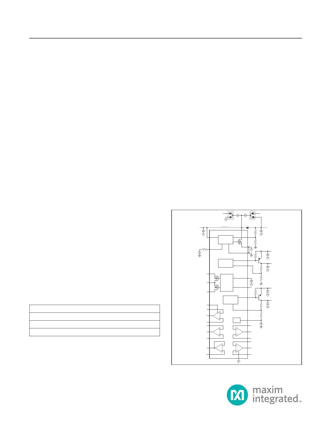
Minimal Operating Circuit
VCN VCP
VIN
LX
IN
STEP-UP
CONTROLLER
FB
COMP
MAX1518A
GATE-ON
CONTROLLER
PGND
AGND
DRVP
FBP
SRC
COM
DRN
SWITCH
CONTROL
SUP
NEG1
OUT1 OP1
POS1
NEG2
GATE-OFF
CONTROLLER
REF
DEL
CTL
DRVN
FBN
REF
NEG4
OUT2 OP2
POS2
OP4 OUT4
POS4
NEG5
OUT3
OP3
POS3
OP5 OUT5
BGND
POS5
VMAIN
VCP
VGON
VCN
VGOFF
19-4019; Rev 1; 10/14
1 page 
MAX1516A/MAX1517A/
MAX1518A
TFT-LCD DC-DC Converters with
Operational Amplifiers
Electrical Characteristics
(VIN = 3V, VSUP = 8V, PGND = AGND = BGND = 0, IREF = 25μA, TA = -40°C to +85°C. unless otherwise noted.) (Note 1)
PARAMETER
SYMBOL
CONDITIONS
IN Supply Range
IN Undervoltage-Lockout
Threshold
VIN
VUVLO
VIN rising, typical hysteresis = 150mV
IN Quiescent Current
VFB = VFBP = 1.4V, VFBN = 0,
LX not switching
IIN VFB = 1.1V, VFBP = 1.4V, VFBN = 0,
LX switching
REF Output Voltage
MAIN STEP-UP REGULATOR
-2µA < IREF < 50µA, VIN = 2.6V to 5.5V
Output Voltage Range
Operating Frequency
FB Regulation Voltage
FB Line Regulation
FB Input Bias Current
FB Transconductance
LX On-Resistance
LX Current Limit
OPERATIONAL AMPLIFIERS
VMAIN
fOSC
VFB
RLX(ON)
ILIM
No load
VIN = 2.6V to 5.5V
VFB = 1.4V
ΔICOMP = 5µA
VFB = 1V, duty cycle = 65%
SUP Supply Range
SUP Supply Current
VSUP
ISUP
Buffer configuration,
VPOS_ = 4V, no load
MAX1518A
MAX1517A
MAX1516A
Input Offset Voltage
Input Common-Mode Range
Output Voltage Swing, High
Output Voltage Swing, Low
Short-Circuit Current
VOS
VCM
VOH
VOL
(VNEG_, VPOS_, VOUT_) @ VSUP / 2
IOUT_ = 100µA
IOUT_ = 5mA
IOUT_ = -100µA
IOUT_ = -5mA
To VSUP / 2
Source
Sink
Output Source and Sink Current
(VNEG_ , VPOS_, VOUT_) @ VSUP / 2,
|ΔVOS| < 10mV (|ΔVOS| < 30mV for OUT3)
GATE-ON LINEAR-REGULATOR CONTROLLER
FBP Regulation Voltage
VFBP IDRVP = 100µA
MIN
2.6
2.265
1.222
VIN
1020
1.212
-40
75
2.5
4.5
0
VSUP - 15
VSUP - 150
50
50
40
1.218
MAX
5.5
UNITS
V
2.715
V
0.8
11
1.269
mA
V
13
1380
1.250
±0.15
+40
300
250
3.5
V
kHz
V
%/ V
nA
µS
mΩ
A
13.0
4.8
3.0
1.1
12
VSUP
15
150
V
mA
mV
V
mV
mV
mA
mA
1.269
V
www.maximintegrated.com
Maxim Integrated │ 5
5 Page 
MAX1516A/MAX1517A/
MAX1518A
TFT-LCD DC-DC Converters with
Operational Amplifiers
Pin Description (continued)
NAME
PIN
MAX1516A MAX1517A MAX1518A
FUNCTION
20 N.C.
N.C.
OUT5
Operational-Amplifier 5 Output. Not internally connected for the MAX1517A and
MAX1516A.
21 LX
LX
LX
n-Channel Power MOSFET Drain and Switching Node. Connect the inductor and
Schottky diode to LX and minimize the trace area for lowest EMI.
22 IN IN IN Supply Voltage Input. IN can range from 2.6V to 5.5V.
Step-Up Regulator Feedback Input. Regulates to 1.236V (nominal). Connect a
23 FB FB FB resistive voltage-divider from the output (VMAIN) to FB to analog ground (AGND).
Place the divider within 5mm of FB.
Step-Up Regulator Error-Amplifier Compensation Point. Connect a series RC from
24 COMP COMP COMP COMP to AGND. See the Loop Compensation section for component selection
guidelines.
25 FBP
FBP
FBP
Gate-On Linear-Regulator Feedback Input. FBP regulates to 1.25V (nominal).
Connect FBP to the center of a resistive voltage-divider between the regulator
output and AGND to set the gate-on linear-regulator output voltage. Place the
resistive voltage-divider close to the pin.
26 DRVP
DRVP
DRVP
Gate-On Linear-Regulator Base Drive. Open drain of an internal n-channel
MOSFET. Connect DRVP to the base of an external pnp pass transistor. See the
Pass-Transistor Selection section.
27 FBN
FBN
FBN
Gate-Off Linear-Regulator Feedback Input. FBN regulates to 250mV (nominal).
Connect FBN to the center of a resistive voltage-divider between the regulator
output and REF to set the gate-off linear-regulator output voltage. Place the
resistive voltage-divider close to the pin.
28 DRVN
29 DEL
30 CTL
31 DRN
32 COM
DRVN
DEL
CTL
DRN
COM
DRVN
DEL
CTL
DRN
COM
Gate-Off Linear-Regulator Base Drive. Open drain of an internal p-channel
MOSFET. Connect DRVN to the base of an external npn pass transistor. See the
Pass-Transistor Selection section.
High-Voltage Switch Delay Input. Connect a capacitor from DEL to AGND to set the
high-voltage switch startup delay.
High-Voltage Switch Control Input. When CTL is high, the high-voltage switch
between COM and SRC is on and the high-voltage switch between COM and DRN
is off. When CTL is low, the high-voltage switch between COM and SRC is off
and the high-voltage switch between COM and DRN is on. CTL is inhibited by the
undervoltage lockout and when the voltage on DEL is less than 1.25V.
Switch Input. Drain of the internal high-voltage back-to-back p-channel MOSFETs
connected to COM.
Internal High-Voltage MOSFET Switch Common Terminal. Do not allow the voltage
on COM to exceed VSRC.
www.maximintegrated.com
Maxim Integrated │ 11
11 Page | ||
| Páginas | Total 29 Páginas | |
| PDF Descargar | [ Datasheet MAX1518A.PDF ] | |
Hoja de datos destacado
| Número de pieza | Descripción | Fabricantes |
| MAX1518 | (MAX1516 - MAX1518) TFT-LCD DC-DC Converters | Maxim Integrated Products |
| MAX1518A | TFT-LCD DC-DC Converters | Maxim Integrated |
| MAX1518B | TFT-LCD DC-DC Converter | Maxim Integrated Products |
| Número de pieza | Descripción | Fabricantes |
| SLA6805M | High Voltage 3 phase Motor Driver IC. |
Sanken |
| SDC1742 | 12- and 14-Bit Hybrid Synchro / Resolver-to-Digital Converters. |
Analog Devices |
|
DataSheet.es es una pagina web que funciona como un repositorio de manuales o hoja de datos de muchos de los productos más populares, |
| DataSheet.es | 2020 | Privacy Policy | Contacto | Buscar |