|
|
|
PDF FDMS3664S Data sheet ( Hoja de datos )
| Número de pieza | FDMS3664S | |
| Descripción | MOSFET ( Transistor ) | |
| Fabricantes | Fairchild Semiconductor | |
| Logotipo | ||
Hay una vista previa y un enlace de descarga de FDMS3664S (archivo pdf) en la parte inferior de esta página. Total 16 Páginas | ||
|
No Preview Available !
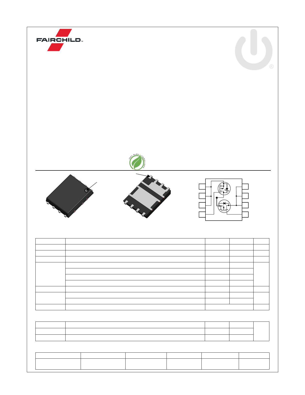
FDMS3664S
PowerTrench® Power Stage
January 2015
Asymmetric Dual N-Channel MOSFET
Features
General Description
Q1: N-Channel
Max rDS(on) = 8 mΩ at VGS = 10 V, ID = 13 A
Max rDS(on) = 11 mΩ at VGS = 4.5 V, ID = 11 A
Q2: N-Channel
Max rDS(on) = 2.6 mΩ at VGS = 10 V, ID = 25 A
Max rDS(on) = 3.2 mΩ at VGS = 4.5 V, ID = 22 A
Low inductance packaging shortens rise/fall times, resulting in
lower switching losses
MOSFET integration enables optimum layout for
lower circuit inductance and reduced switch node
ringing
RoHS Compliant
This device includes two specialized N-Channel MOSFETs in a
dual PQFN package. The switch node has been internally
connected to enable easy placement and routing of synchronous
buck converters. The control MOSFET (Q1) and synchronous
SyncFETTM (Q2) have been designed to provide optimal power
efficiency.
Applications
Computing
Communications
General Purpose Point of Load
Notebook VCORE
Pin 1
Pin 1
G1
D1
D1
D1
D1
S2 5
Q2
4 D1
PHASE
(S1/D2)
G2
S2
S2
S2
Top Power 56 Bottom
MOSFET Maximum Ratings TA = 25 °C unless otherwise noted
S2 6
S2 7
G2 8
PHASE
3 D1
2 D1
Q1 1 G1
Symbol
VDS
VDSt
VGS
ID
EAS
PD
TJ, TSTG
Parameter
Drain to Source Voltage
Drain to Source Transient Voltage ( tTransient < 100 ns)
Gate to Source Voltage
Drain Current -Continuous (Package limited)
-Continuous (Silicon limited)
-Continuous
-Pulsed
Single Pulse Avalanche Energy
Power Dissipation for Single Operation
Power Dissipation for Single Operation
Operating and Storage Junction Temperature Range
(Note 3)
TC = 25 °C
TC = 25 °C
TA = 25 °C
TA = 25 °C
TA = 25 °C
Q1 Q2
30 30
33 33
±20 ±12
30 60
60
131a
118
251b
40
334
2.21a
11c
100
485
2.51b
11d
-55 to +150
Units
V
V
V
A
mJ
W
°C
Thermal Characteristics
RθJA
RθJA
RθJC
Thermal Resistance, Junction to Ambient
Thermal Resistance, Junction to Ambient
Thermal Resistance, Junction to Case
Package Marking and Ordering Information
571a
1251c
2.9
501b
1201d
2.3
°C/W
Device Marking
22CF
10OD
Device
FDMS3664S
Package
Power 56
Reel Size
13 ”
Tape Width
12 mm
Quantity
3000 units
©2012 Fairchild Semiconductor Corporation
FDMS3664S Rev.C5
1
www.fairchildsemi.com
1 page 
Typical Characteristics (Q1 N-Channel) TJ = 25 °C unless otherwise noted
10
ID = 13 A
8
6
4
VDD = 10 V
VDD = 15 V
VDD = 20 V
2000
1000
100
Ciss
Coss
2
0
0 5 10 15 20 25
Qg, GATE CHARGE (nC)
Figure 7. Gate Charge Characteristics
Crss
f = 1 MHz
VGS = 0 V
10
0.1
1
10
VDS, DRAIN TO SOURCE VOLTAGE (V)
30
Figure8. Capacitance vsDrain
to Source Voltage
100
TJ = 25 oC
10
TJ = 100 oC
1
0.001
TJ = 125 oC
0.01 0.1 1 10
tAV, TIME IN AVALANCHE (ms)
100
Figure9. UnclampedInductive
Switching Capability
100
100 μs
10
1 THIS AREA IS
LIMITED BY rDS(on)
SINGLE PULSE
0.1 TJ = MAX RATED
RθJA = 125 oC/W
TA = 25 oC
0.01
0.01
0.1
1
1 ms
10 ms
100 ms
1s
10 s
DC
10 100200
VDS, DRAIN to SOURCE VOLTAGE (V)
Figure 11. Forward Bias Safe
Operating Area
80
RθJC = 2.9 oC/W
60 VGS = 10 V
40 VGS = 4.5 V
20
Limited by Package
0
25 50 75 100 125 150
TC, CASE TEMPERATURE (oC)
Figure 10. Maximum Continuous Drain
Current vs Case Temperature
1000
100
SINGLE PULSE
RθJA = 125 oC/W
10
1
0.110-4 10-3 10-2 10-1
1
10
t, PULSE WIDTH (sec)
100 1000
Figure 12. Single Pulse Maximum
Power Dissipation
©2012 Fairchild Semiconductor Corporation
FDMS3664S Rev.C5
5
www.fairchildsemi.com
5 Page 
Application Information
1. Switch Node Ringing Suppression
Fairchild’s Power Stage products incorporate a proprietary design* that minimizes the peak overshoot, ringing voltage on the switch
node (PHASE) without the need of any external snubbing components in a buck converter. As shown in the figure 29, the Power Stage
solution rings significantly less than competitor solutions under the same set of test conditions.
Power Stage Device
Competitors solution
Figure 29. Power Stage phase node rising edge, High Side Turn on
*Patent Pending
©2012 Fairchild Semiconductor Corporation
FDMS3664S Rev.C5
11
www.fairchildsemi.com
11 Page | ||
| Páginas | Total 16 Páginas | |
| PDF Descargar | [ Datasheet FDMS3664S.PDF ] | |
Hoja de datos destacado
| Número de pieza | Descripción | Fabricantes |
| FDMS3664S | MOSFET ( Transistor ) | Fairchild Semiconductor |
| Número de pieza | Descripción | Fabricantes |
| SLA6805M | High Voltage 3 phase Motor Driver IC. |
Sanken |
| SDC1742 | 12- and 14-Bit Hybrid Synchro / Resolver-to-Digital Converters. |
Analog Devices |
|
DataSheet.es es una pagina web que funciona como un repositorio de manuales o hoja de datos de muchos de los productos más populares, |
| DataSheet.es | 2020 | Privacy Policy | Contacto | Buscar |