|
|
|
PDF FDG8842CZ Data sheet ( Hoja de datos )
| Número de pieza | FDG8842CZ | |
| Descripción | MOSFET ( Transistor ) | |
| Fabricantes | Fairchild Semiconductor | |
| Logotipo | ||
Hay una vista previa y un enlace de descarga de FDG8842CZ (archivo pdf) en la parte inferior de esta página. Total 9 Páginas | ||
|
No Preview Available !
FDG8842CZ
Complementary PowerTrench® MOSFET
April 2007
tm
Q1:30V,0.75A,0.4Ω; Q2:–25V,–0.41A,1.1Ω
Features
Q1: N-Channel
Max rDS(on) = 0.4Ω at VGS = 4.5V, ID = 0.75A
Max rDS(on) = 0.5Ω at VGS = 2.7V, ID = 0.67A
Q2: P-Channel
Max rDS(on) = 1.1Ω at VGS = –4.5V, ID = –0.41A
Max rDS(on) = 1.5Ω at VGS = –2.7V, ID = –0.25A
Very low level gate drive requirements allowing direct
operation in 3V circuits(VGS(th) <1.5V)
Very small package outline SC70-6
General Description
These N & P-Channel logic level enhancement mode field effect
transistors are produced using Fairchild’s proprietary, high cell
density, DMOS technology. This very high density process is
especially tailored to minimize on-state resistance. This
device has been designed especially for low voltage applica-
tions as a replacement for bipolar digital transistors and small
signal MOSFETs. Since bias resistors are not required, this dual
digital FET can replace several different digital transistors, with
different bias resistor values.
RoHS Compliant
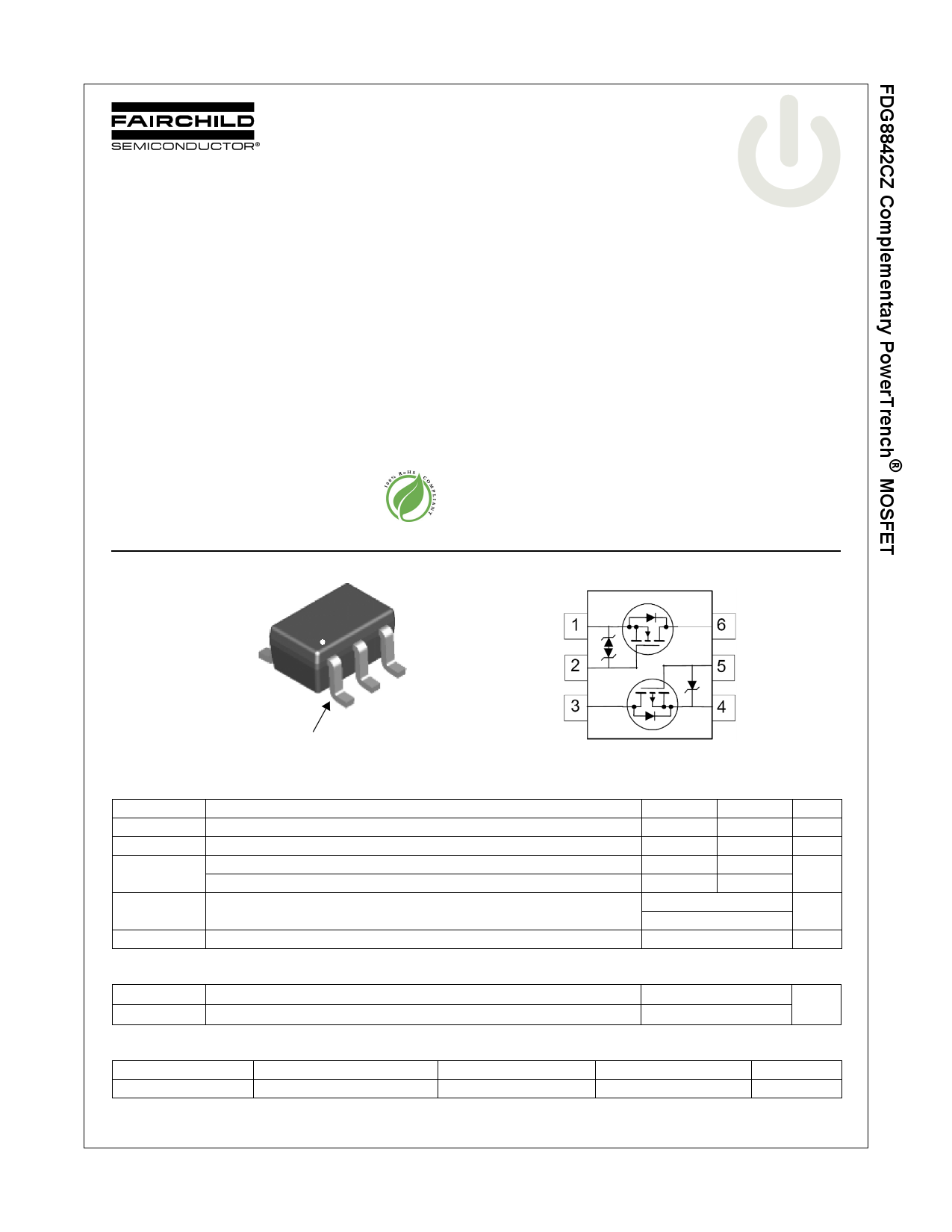
S2
G2
D1
SC70-6
Pin 1
D2
G1
S1
S1 Q1
G1
D2 Q2
D1
G2
S2
MOSFET Maximum Ratings TA = 25°C unless otherwise noted
Symbol
VDS
VGS
ID
PD
Parameter
Drain to Source Voltage
Gate to Source Voltage
Drain Current
-Continuous
-Pulsed
Power Dissipation for Single Operation
TJ, TSTG
Operating and Storage Junction Temperature Range
Thermal Characteristics
RθJA
RθJA
Thermal Resistance, Junction to Ambient Single operation
Thermal Resistance, Junction to Ambient Single operation
Package Marking and Ordering Information
Device Marking
.42
Device
FDG8842CZ
Reel Size
7”
(Note 1a)
(Note 1b)
Q1 Q2
30 –25
±12 –8
0.75 –0.41
2.2 –1.2
0.36
0.30
–55 to +150
Units
V
V
A
W
°C
(Note 1a)
(Note 1b)
350
415
°C/W
Tape Width
8mm
Quantity
3000 units
©2007 Fairchild Semiconductor Corporation
FDG8842CZ Rev.B
1
www.fairchildsemi.com
1 page 
Typical Characteristics (Q1 N-Channel)TJ = 25°C unless otherwise noted
5
ID = 0.22A
4
3 VDD = 5V
2
VDD = 10V
VDD = 15V
200
100
10
Ciss
Coss
Crss
1
0
0.0 0.2 0.4 0.6 0.8 1.0 1.2 1.4
Qg, GATE CHARGE(nC)
Figure 7. Gate Charge Characteristics
f = 1MHz
VGS = 0V
01.1 1
10
VDS, DRAIN TO SOURCE VOLTAGE (V)
Figure8. CapacitancevsDrain
to Source Voltage
30
4
1
LIMITED
r DS(on)
100μs
1ms
0.1 10ms
SINGLE PULSE
0.01
TJ = MAX RATED
RθJA = 415OC/W
TA = 25OC
0.005
0.1
1
100ms
1s
DC
10 100
VDS, DRAIN to SOURCE VOLTAGE (V)
Figure 9. Forward Bias Safe
Operating Area
50
SINGLE PULSE
RθJA= 415OC/W
10 TA = 25OC
1
0.1
0.0001 0.001 0.01 0.1 1 10 100 1000
t, PULSE WIDTH (s)
Figure 10. Single Pulse Maximum Power
Dissipation
1
DUTY CYCLE-DESCENDING ORDER
D = 0.5
0.2
0.1
0.05
0.1
0.02
0.01
0.01 SINGLE PULSE
PDM
t1
t2
NOTES:
DUTY FACTOR: D = t1/t2
PEAK TJ = PDM x ZθJA x RθJA + TA
RθJA = 415oC/W
0.0001
0.001
0.01 0.1
1
t, RECTANGULAR PULSE DURATION (s)
10
Figure 11. Transient Thermal Response Curve
100 1000
©2007 Fairchild Semiconductor Corporation
FDG8842CZ Rev.B
5
www.fairchildsemi.com
5 Page | ||
| Páginas | Total 9 Páginas | |
| PDF Descargar | [ Datasheet FDG8842CZ.PDF ] | |
Hoja de datos destacado
| Número de pieza | Descripción | Fabricantes |
| FDG8842CZ | MOSFET ( Transistor ) | Fairchild Semiconductor |
| Número de pieza | Descripción | Fabricantes |
| SLA6805M | High Voltage 3 phase Motor Driver IC. |
Sanken |
| SDC1742 | 12- and 14-Bit Hybrid Synchro / Resolver-to-Digital Converters. |
Analog Devices |
|
DataSheet.es es una pagina web que funciona como un repositorio de manuales o hoja de datos de muchos de los productos más populares, |
| DataSheet.es | 2020 | Privacy Policy | Contacto | Buscar |