|
|
|
PDF AD7829-1 Data sheet ( Hoja de datos )
| Número de pieza | AD7829-1 | |
| Descripción | 8-Channel ADC | |
| Fabricantes | Analog Devices | |
| Logotipo | ||
Hay una vista previa y un enlace de descarga de AD7829-1 (archivo pdf) en la parte inferior de esta página. Total 21 Páginas | ||
|
No Preview Available !
3 V/5 V, 2 MSPS, 8-Bit, 8-Channel ADC
AD7829-1
FEATURES
8-bit half-flash ADC with 420 ns conversion time
Eight single-ended analog input channels
Available with input offset adjust
On-chip track-and-hold
SNR performance given for input frequencies
up to10 MHz
On-chip reference (2.5 V)
Automatic power-down at the end of conversion
Wide operating supply range
3 V ± 10% and 5 V ± 10%
Input ranges
0 V to 2 V p-p, VDD = 3 V ± 10%
0 V to 2.5 V p-p, VDD = 5 V ± 10%
Flexible parallel interface with EOC pulse to allow
stand-alone operation
APPLICATIONS
Data acquisition systems, DSP front ends
Disk drives
Mobile communication systems, subsampling
applications
GENERAL DESCRIPTION
The AD7829-1 is a high speed 8-channel, microprocessor-
compatible, 8-bit analog-to-digital converter with a maximum
throughput of 2 MSPS. The AD7829-1 contains an on-chip
reference of 2.5 V (2% tolerance); a track-and-hold amplifier;
a 420 ns, 8-bit half-flash ADC; and a high speed parallel
interface. The converter can operate from a single 3 V ± 10%
and 5 V ± 10% supply.
The AD7829-1 combines the convert start and power-down
functions at one pin, that is, the CONVST pin. This allows a
unique automatic power-down at the end of a conversion to be
implemented. The logic level on the CONVST pin is sampled
after the end of a conversion when an EOC (end of conversion)
signal goes high, and if it is logic low at that point, the ADC is
powered down. The parallel interface is designed to allow easy
interfacing to microprocessors and DSPs. Using only address
decoding logic, the parts are easily mapped into the microprocessor
address space.
The EOC pulse allows the ADCs to be used in a stand-alone
manner (see the Parallel Interface section).
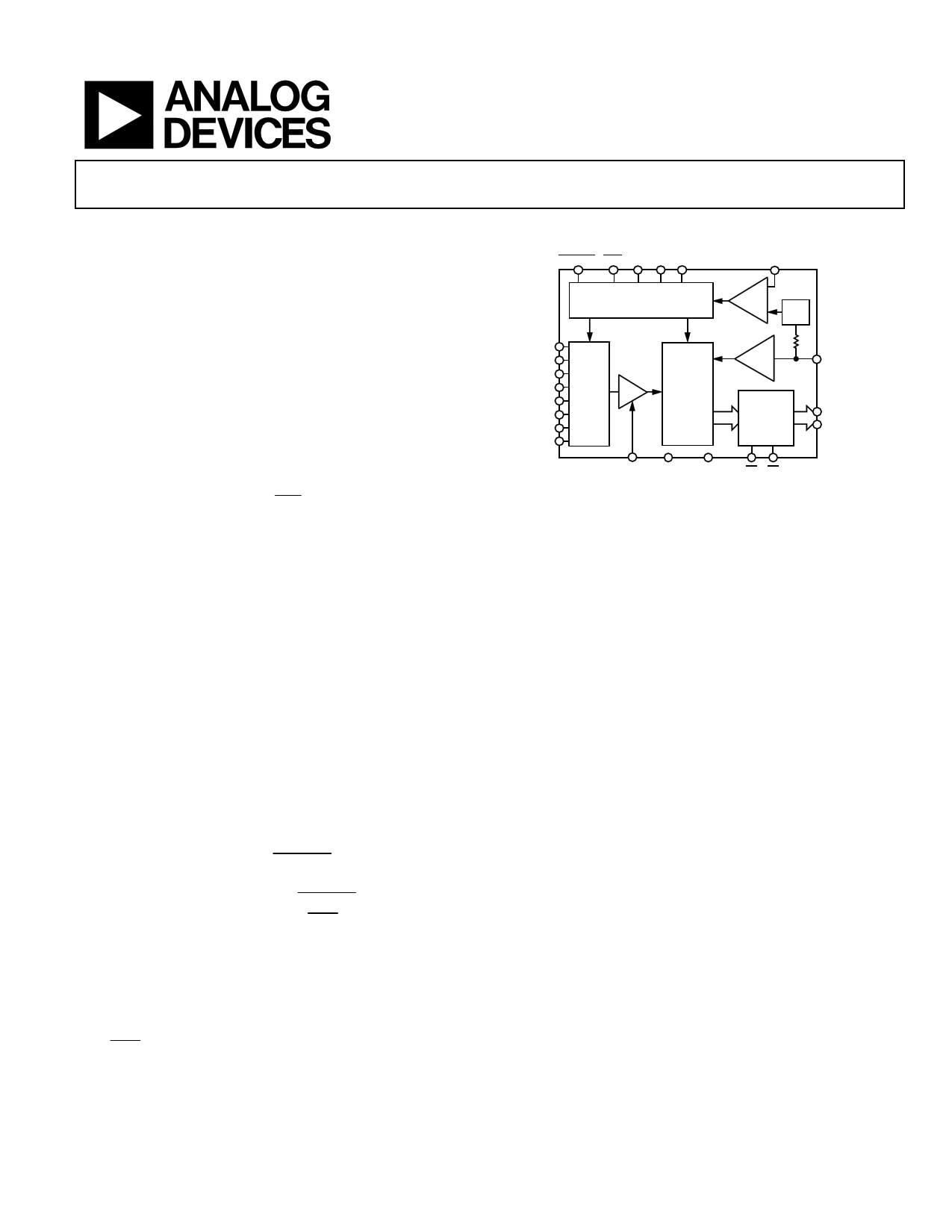
FUNCTIONAL BLOCK DIAGRAM
CONVST EOC A0 A1 A2
VDD
CONTROL
LOGIC
COMP
2.5V
REF
VIN1
VIN2
VIN3
VIN4
VIN5
VIN6
VIN7
VIN8
INPUT
MUX
T/H
8-BIT
HALF
FLASH
ADC
BUF
PARALLEL
PORT
VMID AGND DGND
Figure 1.
CS RD
VREF IN/OUT
DB7
DB0
The AD7829-1 is available in a 28-lead, wide body, small outline
IC (SOIC_W) and a 28-lead thin shrink small outline package
(TSSOP).
PRODUCT HIGHLIGHTS
1. Fast Conversion Time. The AD7829-1 has a conversion
time of 420 ns. Faster conversion times maximize the DSP
processing time in a real-time system.
2. Analog Input Span Adjustment. The VMID pin allows the
user to offset the input span. This feature can reduce the
requirements of single-supply op amps and take into
account any system offsets.
3. FPBW (Full Power Bandwidth) of Track-and-Hold. The
track-and-hold amplifier has excellent high frequency
performance. The AD7829-1 is capable of converting full-
scale input signals up to a frequency of 10 MHz, making
the parts ideally suited to subsampling applications.
4. Channel Selection. Channel selection is made without the
necessity of writing to the part.
Rev. 0
Information furnished by Analog Devices is believed to be accurate and reliable. However, no
responsibility is assumed by Analog Devices for its use, nor for any infringements of patents or other
rights of third parties that may result from its use. Specifications subject to change without notice. No
license is granted by implication or otherwise under any patent or patent rights of Analog Devices.
Trademarksandregisteredtrademarksarethepropertyoftheirrespectiveowners.
One Technology Way, P.O. Box 9106, Norwood, MA 02062-9106, U.S.A.
Tel: 781.329.4700
www.analog.com
Fax: 781.461.3113
©2006 Analog Devices, Inc. All rights reserved.
1 page 
AD7829-1
Parameter
LOGIC OUTPUTS
Output High Voltage, VOH
Output Low Voltage, VOL
High Impedance Leakage Current
High Impedance Capacitance
CONVERSION RATE
Track/Hold Acquisition Time
Conversion Time
POWER SUPPLY REJECTION
VDD ± 10%
POWER REQUIREMENTS
VDD
VDD
IDD
Normal Operation
Power-Down
Power Dissipation
Normal Operation
Power-Down
200 kSPS
500 kSPS
Version B
4
2.4
0.4
0.2
±1
10
200
420
±1
4.5
5.5
2.7
3.3
12
5
0.2
36
9.58
23.94
1 See the Terminology section of this data sheet.
2 Refer to the Analog Input section for an explanation of the analog input(s).
Unit
V min
V min
V max
V max
μA max
pF max
ns max
ns max
LSB max
V min
V max
V min
V max
mA max
μA max
μA typ
mW max
mW typ
mW typ
Test Conditions/Comments
ISOURCE = 200 μA
VDD = 5 V ± 10%
VDD = 3 V ± 10%
ISINK = 200 μA
VDD = 5 V ± 10%
VDD = 3 V ± 10%
See Circuit Description section
5 V ± 10%; for specified performance
3 V ± 10%; for specified performance
8 mA typically
Logic inputs = 0 V or VDD
VDD = 3 V
Typically 24 mW
Rev. 0 | Page 4 of 20
5 Page 
AD7829-1
CIRCUIT INFORMATION
CIRCUIT DESCRIPTION
The AD7829-1 consists of a track-and-hold amplifier followed
by a half-flash analog-to-digital converter. These devices use a
half-flash conversion technique where one 4-bit flash ADC is
used to achieve an 8-bit result. The 4-bit flash ADC contains a
sampling capacitor followed by 15 comparators that compare
the unknown input to a reference ladder to achieve a 4-bit result.
This first flash, that is, coarse conversion, provides the four
MSBs. For a full 8-bit reading to be realized, a second flash,
that is, a fine conversion, must be performed to provide the four
LSBs. The 8-bit word is then placed on the data output bus.
Figure 4 and Figure 5 show simplified schematics of the ADC.
When the ADC starts a conversion, the track-and-hold goes
into hold mode and holds the analog input for 120 ns. This is
the acquisition phase as shown in Figure 4, when Switch 2 is in
Position A. At the point when the track-and-hold returns to its
track mode, this signal is sampled by the sampling capacitor as
Switch 2 moves into Position B. The first flash occurs at this
instant and is then followed by the second flash. Typically, the
first flash is complete after 100 ns, that is, at 220 ns, while the
end of the second flash and, hence, the 8-bit conversion result,
is available at 330 ns (minimum). The maximum conversion
time is 420 ns. As shown in Figure 6, the track-and-hold returns
to track mode after 120 ns and starts the next acquisition before
the end of the current conversion. Figure 8 shows the ADC
transfer function.
REFERENCE
R16
A SW2
R15
VIN T/H 1
B SAMPLING
HOLD
CAPACITOR
R14
R13
15
14
13
TIMING AND
CONTROL
LOGIC
R1
1
Figure 4. ADC Acquisition Phase
D7
D6
D5
D4
D3
D2
D1
D0
REFERENCE
R16
A SW2
R15
VIN T/H 1
B
HOLD
SAMPLING
CAPACITOR
R14
R13
15
14
13
TIMING AND
CONTROL
LOGIC
R1
1
D7
D6
D5
D4
D3
D2
D1
D0
Figure 5. ADC Conversion Phase
TRACK
120ns
HOLD
CONVST
t2
EOC
t1
TRACK
HOLD
CS
t3
RD
DB0 TO DB7
VALID
DATA
Figure 6. Track-and-Hold Timing
TYPICAL CONNECTION DIAGRAM
Figure 7 shows a typical connection diagram for the AD7829-1.
The AGND and DGND are connected together at the device for
good noise suppression. The parallel interface is implemented
using an 8-bit data bus. The end of conversion signal (EOC) idles
high, the falling edge of CONVST initiates a conversion, and at
the end of conversion the falling edge of EOC is used to initiate
an interrupt service routine (ISR) on a microprocessor (see the
Parallel Interface section). VREF IN/OUT and VMID are connected to a
voltage source, such as the AD780, while VDD is connected to a
voltage source that can vary from 4.5 V to 5.5 V (see Table 5 in
the Analog Input section). When VDD is first connected, the
AD7829-1 powers up in a low current mode, that is, power-down.
Ensure that the CONVST line is not floating when VDD is applied,
because this can put the AD7829-1 into an unknown state.
Rev. 0 | Page 10 of 20
11 Page | ||
| Páginas | Total 21 Páginas | |
| PDF Descargar | [ Datasheet AD7829-1.PDF ] | |
Hoja de datos destacado
| Número de pieza | Descripción | Fabricantes |
| AD7829-1 | 8-Channel ADC | Analog Devices |
| Número de pieza | Descripción | Fabricantes |
| SLA6805M | High Voltage 3 phase Motor Driver IC. |
Sanken |
| SDC1742 | 12- and 14-Bit Hybrid Synchro / Resolver-to-Digital Converters. |
Analog Devices |
|
DataSheet.es es una pagina web que funciona como un repositorio de manuales o hoja de datos de muchos de los productos más populares, |
| DataSheet.es | 2020 | Privacy Policy | Contacto | Buscar |