|
|
|
PDF XC6211 Data sheet ( Hoja de datos )
| Número de pieza | XC6211 | |
| Descripción | 300mA High Speed LDO Regulators | |
| Fabricantes | Torex Semiconductor | |
| Logotipo | ||
Hay una vista previa y un enlace de descarga de XC6211 (archivo pdf) en la parte inferior de esta página. Total 30 Páginas | ||
|
No Preview Available !
XC6219/XC6211 Series
300mA High Speed LDO Regulators with ON/OFF Switch
ETR0307_009
■GENERAL DESCRIPTION
The XC6219/XC6211 series are highly accurate, low noise, CMOS LDO Voltage Regulators. Offering low output noise, high
ripple rejection ratio, low dropout and very fast turn-on times, the XC6219/XC6211 series is ideal for today’s cutting edge
mobile phone.
Internally the XC6219/XC6211 includes a reference voltage source, error amplifiers, driver transistors, current limiters and
phase compensators. The XC6219/XC6211’s current limiters' foldback circuit also operates as a short protect for the output
current limiter and. the output pin. The output voltage is set by laser trimming. Voltages are selectable in 50mV steps
within a range of 0.9V to 5.0V. The XC6219/XC6211 series is also fully compatible with low ESR ceramic capacitors,
reducing cost and improving output stability. This high level of output stability is maintained even during frequent load
fluctuations, due to the excellent transient response performance and high PSRR achieved across a broad range of
frequencies.
The CE function allows the output of regulator to be turned off, resulting in greatly reduced power consumption.
■APPLICATIONS
●Mobile phones
●Cordless phones, radio communication equipment
●Portable games
●Cameras, Video cameras
●Reference voltage sources
●Battery powered equipment
■FEATURES
Maximum Output Current : 150mA (VOUT<1.75V, A~D type)
240mA (VOUT>1.8V, A~D type)
300mA (VOUT>1.3V, E~H type)
Dropout Voltage
: 200mV @ 100mA
Operating Voltage Range : 2.0V ~ 6.0V
Output Voltage Range : 0.9V ~ 5.0V (0.05V steps)
Highly Accuracy
: +2% (VOUT>1.5V)
+30mV (VOUT≦1.5V)
+1% (VOUT≧3.0V)
Low Power Consumption : 25μA (TYP.)
Standby Current
: Less than 0.1μA (TYP.)
High Ripple Rejection : 65dB @10kHz
Operating Ambient Temperature : -40℃ ~ 85℃
Low ESR Capacitor
: Ceramic capacitor compatible
Ultra Small Packages
: SOT-25
SOT-89-5 (for XC6219 only)
USP-6B (for XC6219 only)
Environmentally Friendly : EU RoHS Compliant, Pb Free
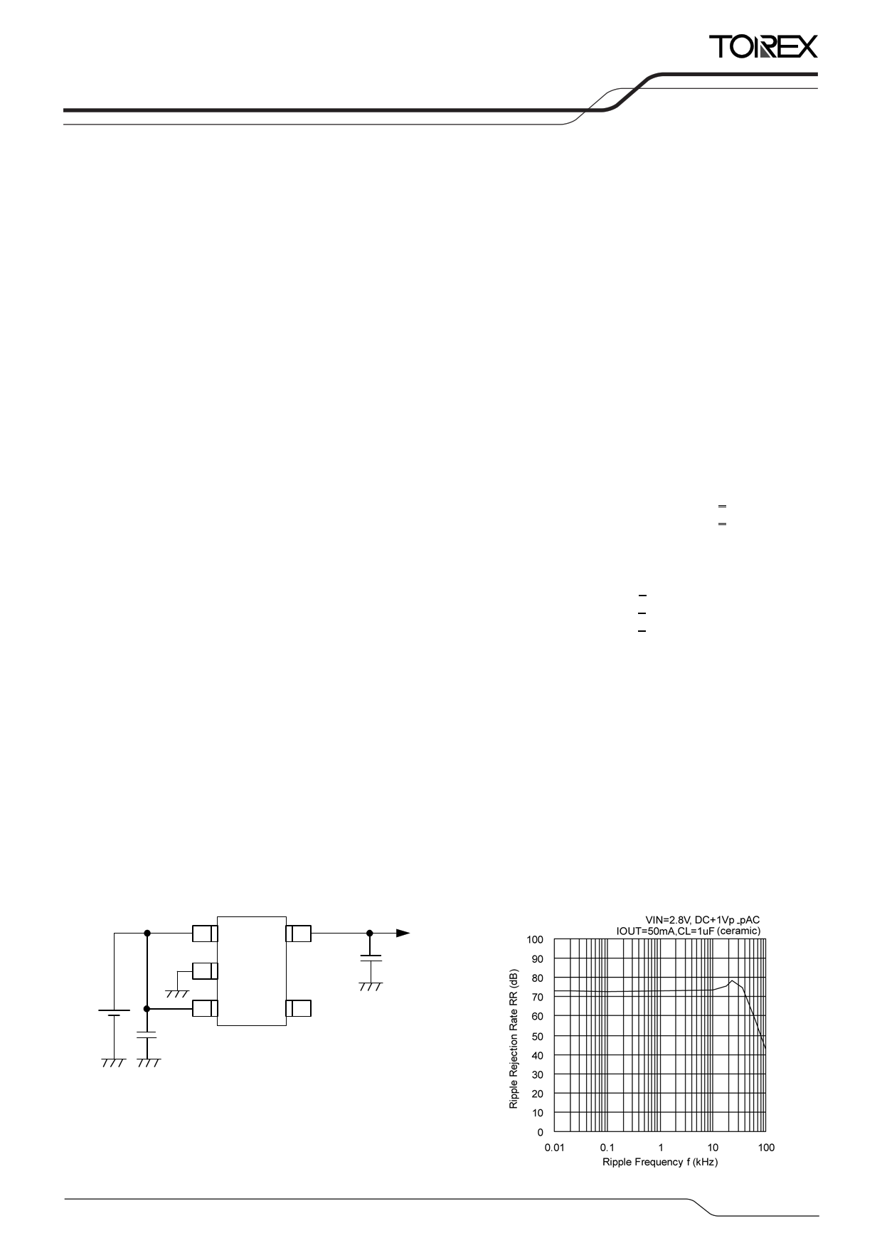
■TYPICAL APPLICATION CIRCUIT
●XC6219 series
■TYPICAL PERFORMANCE
CHARACTERISTICS
●Ripple Rejection Rate
XC6219/XC6211
1 VIN VOUT 5
2 VSS
CL
1μF
3 CE
CIN
1μF
NC 4
SOT-25
1/30
1 page 
XC6219/XC6211
Series
■ELECTRICAL CHARACTERISTICS
●XC6219/XC6211 Type A,B
PARAMETER
Output Voltage (*5)
(2%)
Output Voltage (*6)
(1%)
Maximum Output
Current
SYMBOL
CONDITIONS
VOUT(E) (*3)
IOUT=30mA
IOUTMAX
0.9V≦VOUT(T)≦1.75V
1.8V≦VOUT(T)≦5.0V
Load Regulation
ΔVOUT
1mA≦IOUT≦100mA
Dropout Voltage (*4)
Supply Current
(Type A)
Supply Current
(Type B)
Stand-by Current
Line Regulation
Input Voltage
Output Voltage
Temperature
Characteristics
Power Supply
Rejection Ratio
Current Limiter
Short Circuit Current
CE ‘High’ Level Voltage
CE ‘Low’ Level Voltage
CE ‘High’ Level Current
(Type A)
CE ‘High’ Level Current
(Type B)
Vdif1
Vdif2
IOUT=30mA
IOUT=100mA
IDD
VCE=VIN=VOUT(T)+1.0V
VOUT≦0.95V, VIN=VCE=2.0V
ISTB
ΔVOUT/
(ΔVIN・VOUT)
VIN
VIN=VOUT(T)+1.0V、VCE=VSS
VOUT≦0.95V, VIN=2.0V
VOUT(T)+1.0V≦VIN≦6.0V
VOUT≦0.95V, 2.0V≦VIN≦6.0V
IOUT=30mA
VOUT≦1.75V, IOUT=10mA
-
ΔVOUT/
(ΔTopr・VOUT)
IOUT=30mA
-40℃≦Topr≦85℃
PSRR
Ilim
ISHORT
VCEH
VCEL
VIN=[VOUT(T)+1.0]V+1.0Vp-pAC
VOUT≦1.5, VIN=2.5V+1.0Vp-pAC
IOUT=50mA、f=10kHz
VIN=VOUT(T)+2.0V、VCE=VIN
0.9V≦VOUT(T)≦1.75V
VIN=VOUT(T)+1.0V、VCE=VIN
1.8V≦VOUT(T)≦5.0V
VIN=VOUT(T)+1.0V、 VCE=VIN
VOUT≦1.75V, VIN=VOUT(T)+2.0V
-
-
ICEH
VIN=VCE=VOUT(T)+1.0V
VOUT≦0.95V, VIN=VCE=2.0V
CE ‘Low’ Level Current
ICEL
VIN=VOUT(T)+1.0V、VCE=VSS
VOUT≦0.95V, VIN=2.0V
MIN.
VOUT(T)(*2)
×0.98
VOUT(T)(*2)
×0.99
150
240
-
-
-
-
-
-
-
2
-
-
-
240
-
1.6
-
-0.10
-0.10
-0.10
TYP.
VOUT(T)(*2)
VOUT(T)(*2)
-
-
MAX.
VOUT(T)(*2)
×1.02
VOUT(T)(*2)
×1.01
-
-
Ta=25℃
UNITS CIRCUIT
V①
mA ①
15 50 mV ①
E-1
mV ①
E-2
28 55
μA ②
25 50
0.01
0.10
μA
②
0.01
-
±100
0.20
%/V
①
6V-
-
ppm/℃
①
E-3 - dB ④
300 -
mA ①
300 -
50 - mA ①
- VIN V ①
-
0.25
V
①
- 5.0
μA ②
- 0.10
-
0.10
μA
②
(*1) Unless otherwise stated, VIN=VOUT(T)+1.0V. If VOUT is less than 0.95V, VIN= 2.0V.
(*2) VOUT(T) = Specified output voltage
(*3) VOUT(E) = Effective output voltage
The output voltage when "VOUT(T)+1.0V" is provided at the VIN pin while maintaining a certain IOUT value.
(*4) Vdif={VIN1-VOUT1 }
VOUT1=A voltage equal to 98% of the output voltage whenever an amply stabilized IOUT {VOUT(T)+1.0V} is input.
VIN1=The Input Voltage when VOUT1 appears as Input Voltage is gradually decreased.
(*5)If VOUT(T) is less than 1.45V, VOUT(T) -30mV (MIN.), VOUT(T) + 30mV (MAX.)
(*6)Only for the VOUT(T) is more than 3.0V products.
5/30
5 Page 
■ELECTRICAL CHARACTERISTICS (Continued)
●Specification & Condition by Series
SYMBOL
E-5
CONDITION, RATINGS
INPUT VOLTAGE (V)
OUTPUT VOLTAGE (V)
0.90~0.95
1.00~1.05
1.10~1.15
1.20~1.25
1.30~1.35
1.40~1.45
1.50~1.95
2.00~6.00
VIN
2.5
2.5
2.6
2.7
2.8
2.9
3.0
VOUT(T)+1.0
E-4
MAX. OUTPUT CURRENT
(mA)
MIN
260
260
270
290
300
* VOUT(T)=Nominal output voltage
XC6219/XC6211
Series
11/30
11 Page | ||
| Páginas | Total 30 Páginas | |
| PDF Descargar | [ Datasheet XC6211.PDF ] | |
Hoja de datos destacado
| Número de pieza | Descripción | Fabricantes |
| XC6210 | High Current / High Speed LDO Regulators | Torex Semiconductor |
| XC6211 | 300mA High Speed LDO Regulators | Torex Semiconductor |
| XC6212 | (XC6209 / XC6212) High Speed LDO Regulator | Torex Semiconductor |
| XC6213 | High Speed LDO Regulators | Torex Semiconductor |
| Número de pieza | Descripción | Fabricantes |
| SLA6805M | High Voltage 3 phase Motor Driver IC. |
Sanken |
| SDC1742 | 12- and 14-Bit Hybrid Synchro / Resolver-to-Digital Converters. |
Analog Devices |
|
DataSheet.es es una pagina web que funciona como un repositorio de manuales o hoja de datos de muchos de los productos más populares, |
| DataSheet.es | 2020 | Privacy Policy | Contacto | Buscar |