|
|
|
PDF CD40161BMS Data sheet ( Hoja de datos )
| Número de pieza | CD40161BMS | |
| Descripción | CMOS Synchronous Programmable 4-Bit Counters | |
| Fabricantes | Intersil Corporation | |
| Logotipo | ||
Hay una vista previa y un enlace de descarga de CD40161BMS (archivo pdf) en la parte inferior de esta página. Total 13 Páginas | ||
|
No Preview Available !
CD40160BMS, CD40161BMS, CD40162BMS,
CD40163BMS
December 1992
File Number 3358
CMOS Synchronous Programmable 4-Bit
Counters
CD40160BMS, CD40161BMS, CD40162BMS and
CD40163BMS are 4-bit synchronous programmable
counters. The CLEAR function of the CD40162BMS and
CD40163BMS is synchronous and a low level at the CLEAR
input sets all four outputs low on the next positive CLOCK
edge. The CLEAR function of the CD40160BMS and
CD40161BMS is asychronous and a low level at the CLEAR
input sets all four outputs low regardless of the state of the
CLOCK, LOAD, or ENABLE inputs. A low level at the LOAD
input disables the counter and causes the output to agree
with the setup data after the next CLOCK pulse regardless of
the conditions of the ENABLE inputs.
The carry look-ahead circuitry provides for cascading counters
for n-bit synchronous applications without additional gating.
Instrumental in accomplishing this function are two count-enable
inputs and a carry output (COUT). Counting is enabled when
both PE and TE inputs are high. The TE input is fed forward to
enable COUT. This enabled output produces a positive output
pulses with a duration approximately equal to the positive portion
of the Q1 output. This positive overflow carry pulse can be used
to enable successive cascaded stages. Logic transitions at the
PE or TE inputs may occur when the clock is either high or low.
The CD40160BMS through CD40163BMS types are functionally
equivalent to and pin-compatible with the TTL counter series
74LS160 through 74LS163 respectively.
The CD40160BMS, CD40161BMS, CD40162BMS and
CD40163BMS are supplied in these 16 lead outline packages:
CD40160 CD40161 CD40162 CD40163
Braze Seal DIP H4W H4X H4X H4W
Frit Seal DIP
H1F H1F H1L H1F
Ceramic Flatpack H6P H6W H6P H6W
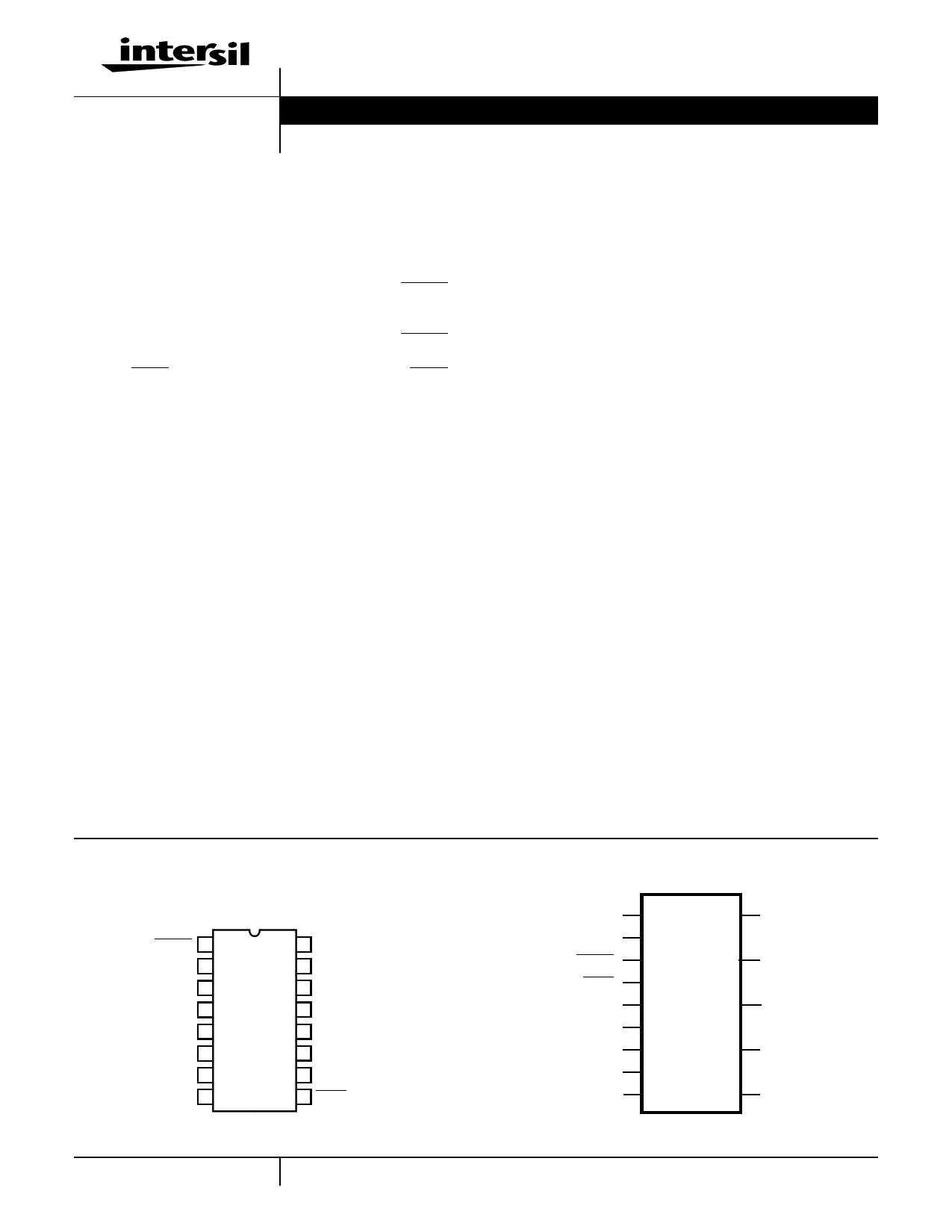
Pinout
CD40160BMS, CD40161BMS, CD40162BMS, CD40163BMS
TOP VIEW
CLEAR 1
CLOCK 2
P1 3
P2 4
P3 5
P4 6
PE 7
VSS 8
16 VDD
15 CARRY OUT
14 Q1
13 Q2
12 Q3
11 Q4
10 TE
9 LOAD
Features
• High-Voltage Types (20V Rating)
• CD40160BMS Decade with Asynchronous Clear
• CD40161BMS Binary with Asynchronous Clear
• CD40162BMS Decade with Synchronous Clear
• CD40163BMS Binary with Synchronous Clear
• Internal Look-Ahead for Fast Counting
• Carry Output for Cascading
• Synchronously Programmable
• Clear Asynchronous Input (CD40160BMS, CD40161BMS)
• Clear Synchronous Input (CD40162BMS, CD40163BMS)
• Synchronous Load Control Input
• Low Power TTL Compatibility
• Standardized Symmetrical Output Characteristics
• 100% Tested for Quiescent Current at 20V
• Maximum Input Current of 1µA at 18V Over Full Package
Temperature Range; 100nA at 18V and +25oC
• Noise Margin (Over Full Package Temperature Range):
- 1V at VDD = 5V
- 2V at VDD = 10V
- 2.5V at VDD = 15V
• 5V, 10V and 15V Parametric Ratings
• Meets All Requirements of JEDEC Tentative Standard No. 13B,
“Standard Specifications for Description of ‘B’ Series CMOS
Devices”
Applications
• Programmable Binary and Decade Counting
• Counter Control/Timers
• Frequency Dividing
Functional Diagram
PE
TE
CLEAR
LOAD
CLOCK
P1
P2
VDD = 16
VSS = 8
P3
P4
7
10
1
9
2
3
4
5
6
14
Q1
13
Q2
12
Q3
11
Q4
15
CARRY
OUT
4-1 CAUTION: These devices are sensitive to electrostatic discharge; follow proper IC Handling Procedures.
1-888-INTERSIL or 321-724-7143 | Copyright © Intersil Corporation 1999
1 page 
CD40160BMS, CD40161BMS, CD40162BMS, CD40163BMS
TABLE 3. ELECTRICAL PERFORMANCE CHARACTERISTICS (Continued)
LIMITS
PARAMETER
Minimum Clear Removal
Time
(CD40160BMS,
CD40161BMS)
SYMBOL
CONDITIONS
TREM VDD = 5V
VDD = 10V
VDD = 15V
NOTES
1, 2, 3
1, 2, 3
1, 2, 3
TEMPERATURE
+25oC
+25oC
+25oC
MIN
-
-
-
MAX
200
100
70
UNITS
ns
ns
ns
NOTES:
1. All voltages referenced to device GND.
2. The parameters listed on Table 3 are controlled via design or process and are not directly tested. These parameters are characterized on initial
design release and upon design changes which would affect these characteristics.
3. CL = 50pF, RL = 200K, Input TR, TF < 20ns.
4. If more than one unit is cascaded, TRCL should be made less than or equal to the sumof the transition time and the fixed propagation delay of
the output of the driving stage for the estimated capacitive load.
TABLE 4. POST IRRADIATION ELECTRICAL PERFORMANCE CHARACTERISTICS
PARAMETER
SYMBOL
CONDITIONS
Supply Current
IDD VDD = 20V, VIN = VDD or GND
N Threshold Voltage
VNTH VDD = 10V, ISS = -10µA
N Threshold Voltage Delta ∆VTN VDD = 10V, ISS = -10µA
P Threshold Voltage
VTP VSS = 0V, IDD = 10µA
P Threshold Voltage Delta ∆VTP VSS = 0V, IDD = 10µA
Functional
F VDD = 18V, VIN = VDD or GND
VDD = 3V, VIN = VDD or GND
Propagation Delay Time
TPHL VDD = 5V
TPLH
NOTES: 1. All voltages referenced to device GND.
2. CL = 50pF, RL = 200K, Input TR, TF < 20ns.
NOTES
1, 4
1, 4
1, 4
1, 4
1, 4
1
TEMPERATURE
+25oC
+25oC
+25oC
+25oC
+25oC
+25oC
1, 2, 3, 4
+25oC
3. See Table 2 for +25oC limit.
4. Read and Record
LIMITS
MIN MAX
- 25
-2.8 -0.2
- ±1
0.2 2.8
- ±1
VOH > VOL <
VDD/2 VDD/2
- 1.35 x
+25oC
Limit
UNITS
µA
V
V
V
V
V
ns
TABLE 5. BURN-IN AND LIFE TEST DELTA PARAMETERS +25oC
PARAMETER
Supply Current - MSI-2
Output Current (Sink)
Output Current (Source)
SYMBOL
IDD
IOL5
IOH5A
DELTA LIMIT
± 1.0µA
± 20% x Pre-Test Reading
± 20% x Pre-Test Reading
TABLE 6. APPLICABLE SUBGROUPS
CONFORMANCE GROUP
MIL-STD-883
METHOD
GROUP A SUBGROUPS
Initial Test (Pre Burn-In)
100% 5004
1, 7, 9
Interim Test 1 (Post Burn-In)
100% 5004
1, 7, 9
Interim Test 2 (Post Burn-In)
100% 5004
1, 7, 9
PDA (Note 1)
100% 5004
1, 7, 9, Deltas
Interim Test 3 (Post Burn-In)
100% 5004
1, 7, 9
PDA (Note 1)
100% 5004
1, 7, 9, Deltas
Final Test
100% 5004
2, 3, 8A, 8B, 10, 11
Group A
Sample 5005
1, 2, 3, 7, 8A, 8B, 9, 10, 11
Group B
Subgroup B-5
Sample 5005
1, 2, 3, 7, 8A, 8B, 9, 10, 11, Deltas
Subgroup B-6
Sample 5005
1, 7, 9
Group D
Sample 5005
1, 2, 3, 8A, 8B, 9
NOTE: 1. 5% Parameteric, 3% Functional; Cumulative for Static 1 and 2.
READ AND RECORD
IDD, IOL5, IOH5A
IDD, IOL5, IOH5A
IDD, IOL5, IOH5A
IDD, IOL5, IOH5A
Subgroups 1, 2, 3, 9, 10, 11
Subgroups 1, 2 3
4-5
5 Page 
CD40160BMS, CD40161BMS, CD40162BMS, CD40163BMS
TN PN
LD
CL CLR
p CL
n
CL
p
n CL
p
n
p CL
np
n
CL
CL
p
n
CL
p
n
CL
QN
QN
FIGURE 12. DETAIL OF FLIP-FLOPS OF CD40160BMS AND CD40161BMS (ASYNCHRONOUS CLEAR)
TN CLR PN
LD
p
n
CL
CL
CL
p CL
np
n
CL
p
p
n
n
CL
CL
p
n
CL
p
n
CL
QN
QN
FIGURE 13. DETAIL OF FLIP-FLOPS OF CD40162BMS AND CD40163BMS (SYNCHRONOUS CLEAR)
4-11
11 Page | ||
| Páginas | Total 13 Páginas | |
| PDF Descargar | [ Datasheet CD40161BMS.PDF ] | |
Hoja de datos destacado
| Número de pieza | Descripción | Fabricantes |
| CD40161BM | (CD40160BM - CD40163BM) Decade Counter with Asynchronous Clear | National Semiconductor |
| CD40161BMS | CMOS Synchronous Programmable 4-Bit Counters | Intersil Corporation |
| Número de pieza | Descripción | Fabricantes |
| SLA6805M | High Voltage 3 phase Motor Driver IC. |
Sanken |
| SDC1742 | 12- and 14-Bit Hybrid Synchro / Resolver-to-Digital Converters. |
Analog Devices |
|
DataSheet.es es una pagina web que funciona como un repositorio de manuales o hoja de datos de muchos de los productos más populares, |
| DataSheet.es | 2020 | Privacy Policy | Contacto | Buscar |