|
|
|
PDF BD62110AEFJ Data sheet ( Hoja de datos )
| Número de pieza | BD62110AEFJ | |
| Descripción | DC Brush Motor Drivers | |
| Fabricantes | ROHM Semiconductor | |
| Logotipo | ||
Hay una vista previa y un enlace de descarga de BD62110AEFJ (archivo pdf) en la parte inferior de esta página. Total 19 Páginas | ||
|
No Preview Available !
Datasheet
36V 1ch
DC Brush Motor Drivers
BD62110AEFJ
General Description
BD62110AEFJ is a built-in 1 channel H-bridge motor
driver for DC brush motors. This driver can facilitate low
power consumption by direct PWM. There are built in
protection circuits in this IC. Each protection circuit
operation contributes to set high reliability.
Features
Single Power Supply Input (rated voltage of 36V)
Rated Output Current (peak):1.0A(2.0A)
Low ON-Resistance DMOS Output
Forward, Reverse, Brake, Open
External PWM Control
Driver for DC Brush Motor
Built-in logic input pull-down resistor
Cross-conduction Prevention Circuit
Thermal Shutdown Circuit (TSD)
Over-current Protection Circuit (OCP)
Under Voltage Lock out Circuit (UVLO)
Over Voltage Lock out Circuit (OVLO)
Ghost Supply Prevention (protects against malfunction
when power supply is disconnected)
Adjacent Pins Short Protection
Inverted Mounting Protection
HTSOP-J8 package
Key Specifications
Power Supply Voltage Range:
Rated Output Current:
Rated Output Current (Peak):
Operating Temperature Range:
Output ON-Resistance:
(Total of upper and lower resistors)
8 to 28 [V]
1.0 [A]
2.0 [A]
-25 to +85 [°C]
1.8 [Ω] (Typ)
Package
HTSOP-J8
W(Typ) x D(Typ)x H(Max)
4.90mm x 6.00mm x 1.00mm
Application
Plain Paper Copier (PPC), Multi-function Printer, Laser
Printer, Inkjet Printer, Photo Printer, FAX, Mini Printer and
etc.
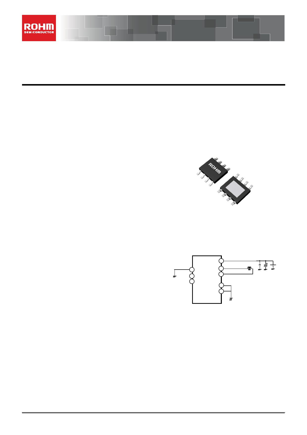
Typical Application Circuit
TEST
IN1
IN2
VCC
OUT1
OUT2
GND
Figure 1. Typical Application Circuit
○Product structure:silicon monolithic integrated circuit
www.rohm.com
© 2016 ROHM Co., Ltd. All rights reserved.
TSZ22111・14・001
○This product has no designed protection against radioactive rays.
1/14
TSZ02201-0P2P0B700870-1-2
2016.05.17 Rev.001
1 page 
BD62110AEFJ
Datasheet
Protection Circuits
(6) Thermal Shutdown (TSD)
This IC has a built-in Thermal Shutdown circuit for thermal protection. When the IC’s chip temperature rises above
175°C (Typ), the motor output becomes OPEN. Also, when the temperature returns to under 150°C (Typ), it
automatically returns to normal operation. However, even when TSD is in operation, if heat is continued to be applied
externally, heat overdrive can lead to destruction.
(7) Over-Current Protection (OCP)
This IC has a built in Over-Current Protection circuit as a provision against destruction when the motor outputs are
shorted to each other or VCC-motor output or motor output-GND is shorted. This circuit latches the motor output to
OPEN condition when the regulated threshold current flows for 4μs (typ). It returns with power reactivation. The
over-current protection circuit aims to prevent the destruction of the IC only from abnormal situations such as when
motor output is shorted and it is not meant to be used as protection or security for the device. Therefore, the device
should not be designed to make use of the function of this circuit. After OCP operation, if abnormal situations
continues and returned by power reactivation or reset of the PS terminal happens repeatedly, then OCP operates
constantly. The IC may generate heat or otherwise deteriorate. When the L value of the wiring is great due to the long
wiring and the over-current flows, the output terminal voltage increases and the absolute maximum values may be
exceeded. As a result, there is a possibility of destruction. Also, when a current flows, which is over the output current
rating and under the OCP detection current, the IC can heat up to over Tjmax=150°C. This can deteriorate the IC.
Therefore, current which exceeds the output rating should not be applied.
(8) Under Voltage Lock Out (UVLO)
This IC has a built-in Under Voltage Lock Out function to prevent false operation such as IC output during power
supply under voltage. When the applied voltage to the VCC terminal goes under 5V (Typ), the motor output is set to
OPEN. This switching voltage has a 1V (Typ) hysteresis to prevent false operation by noise etc.
(9) Over Voltage Lock Out (OVLO)
This IC has a built-in Over Voltage Lock Out function to protect the IC output and the motor during power supply over
voltage. When the applied voltage to the VCC terminal goes over 32V (Typ), the motor output is set to OPEN. This
switching voltage has a 1V (Typ) hysteresis and a 4μs (Typ) mask time to prevent false operation by noise etc.
Although this over voltage locked out circuit is built-in, there is a possibility of destruction if the absolute maximum
value for power supply voltage is exceeded. Therefore, the absolute maximum value should not be exceeded.
(10) Ghost Supply Prevention (protects against malfunction when power supply is disconnected)
If a control signal (IN1, IN2) is applied when there is no power supplied to the IC, there is a function which prevents
false operation by voltage applied via the electrostatic destruction prevention diode from the control input terminal to
the VCC, to this IC or to another IC’s power supply. Therefore, there is no malfunction in the circuit even when
voltage is supplied to these input terminals while there is no power supply.
www.rohm.com
© 2016 ROHM Co., Ltd. All rights reserved.
TSZ22111・15・001
5/15
TSZ02201-0P2P0B700870-1-2
2016.05.17 Rev.001
5 Page 
BD62110AEFJ
Datasheet
Operational Notes – continued
10. Inter-pin Short and Mounting Errors
Ensure that the direction and position are correct when mounting the IC on the PCB. Incorrect mounting may result in
damaging the IC. Avoid nearby pins being shorted to each other especially to ground, power supply and output pin.
Inter-pin shorts could be due to many reasons such as metal particles, water droplets (in very humid environment)
and unintentional solder bridge deposited in between pins during assembly to name a few.
11. Unused Input Pins
Input pins of an IC are often connected to the gate of a MOS transistor. The gate has extremely high impedance and
extremely low capacitance. If left unconnected, the electric field from the outside can easily charge it. The small
charge acquired in this way is enough to produce a significant effect on the conduction through the transistor and
cause unexpected operation of the IC. So unless otherwise specified, unused input pins should be connected to the
power supply or ground line.
12. Regarding the Input Pin of the IC
This monolithic IC contains P+ isolation and P substrate layers between adjacent elements in order to keep them
isolated. P-N junctions are formed at the intersection of the P layers with the N layers of other elements, creating a
parasitic diode or transistor. For example (refer to figure below):
When GND > Pin A and GND > Pin B, the P-N junction operates as a parasitic diode.
When GND > Pin B, the P-N junction operates as a parasitic transistor.
Parasitic diodes inevitably occur in the structure of the IC. The operation of parasitic diodes can result in mutual
interference among circuits, operational faults, or physical damage. Therefore, conditions that cause these diodes to
operate, such as applying a voltage lower than the GND voltage to an input pin (and thus to the P substrate) should
be avoided.
Figure 8. Example of monolithic IC structure
13. Thermal Shutdown Circuit(TSD)
This IC has a built-in thermal shutdown circuit that prevents heat damage to the IC. Normal operation should always
be within the IC’s maximum junction temperature rating. If however the rating is exceeded for a continued period, the
junction temperature (Tj) will rise which will activate the TSD circuit that will turn OFF all output pins. When the Tj falls
below the TSD threshold, the circuits are automatically restored to normal operation.
Note that the TSD circuit operates in a situation that exceeds the absolute maximum ratings and therefore, under no
circumstances, should the TSD circuit be used in a set design or for any purpose other than protecting the IC from
heat damage.
14. Over Current Protection Circuit (OCP)
This IC incorporates an integrated overcurrent protection circuit that is activated when the load is shorted. This
protection circuit is effective in preventing damage due to sudden and unexpected incidents. However, the IC should
not be used in applications characterized by continuous operation or transitioning of the protection circuit.
www.rohm.com
© 2016 ROHM Co., Ltd. All rights reserved.
TSZ22111・15・001
11/15
TSZ02201-0P2P0B700870-1-2
2016.05.17 Rev.001
11 Page | ||
| Páginas | Total 19 Páginas | |
| PDF Descargar | [ Datasheet BD62110AEFJ.PDF ] | |
Hoja de datos destacado
| Número de pieza | Descripción | Fabricantes |
| BD62110AEFJ | DC Brush Motor Drivers | ROHM Semiconductor |
| Número de pieza | Descripción | Fabricantes |
| SLA6805M | High Voltage 3 phase Motor Driver IC. |
Sanken |
| SDC1742 | 12- and 14-Bit Hybrid Synchro / Resolver-to-Digital Converters. |
Analog Devices |
|
DataSheet.es es una pagina web que funciona como un repositorio de manuales o hoja de datos de muchos de los productos más populares, |
| DataSheet.es | 2020 | Privacy Policy | Contacto | Buscar |