|
|
|
PDF 9FGL06 Data sheet ( Hoja de datos )
| Número de pieza | 9FGL06 | |
| Descripción | 6-output 3.3V PCIe Clock Generator | |
| Fabricantes | IDT | |
| Logotipo | ||
Hay una vista previa y un enlace de descarga de 9FGL06 (archivo pdf) en la parte inferior de esta página. Total 19 Páginas | ||
|
No Preview Available !
6-output 3.3V PCIe Clock Generator
9FGL06
DATASHEET
Description
The 9FGL06 devices are 3.3V members of IDT's 3.3V
Full-Featured PCIe family. The devices have 6 output enables
for clock management and support 2 different spread
spectrum levels in addition to spread off. The 9FGL06
supports PCIe Gen1-4 Common Clocked architectures (CC)
and PCIe Separate Reference no-Spread (SRnS) and
Separate Reference Independent Spread (SRIS) clocking
architectures. The 9FGL06P1 can be programmed with a
user-defined power up default SMBus configuration.
Recommended Application
PCIe Gen1-4 clock generation for Riser Cards, Storage,
Networking, JBOD, Communications, Access Points
Output Features
• 6 – 100 MHz Low-Power HCSL (LP-HCSL) DIF pairs
• 9FGL0641 default ZOUT = 100
• 9FGL0651 default ZOUT = 85
• 9FGL06P1 factory programmable defaults
• 1 - 3.3V LVCMOS REF output w/Wake-On-LAN (WOL)
support
• Easy AC-coupling to other logic families, see IDT
application note AN-891
Key Specifications
• PCIe Gen1-2-3-4 CC-compliant
• PCIe Gen2-3 SRIS-compliant
• DIF cycle-to-cycle jitter <50ps
• DIF output-to-output skew <50ps
• DIF 12k-20M phase jitter is <2ps rms when SSC is off
• REF phase jitter is <300fs rms, SSC off, and <1.5ps rms,
SSC is On
• ±100ppm frequency accuracy on all clocks
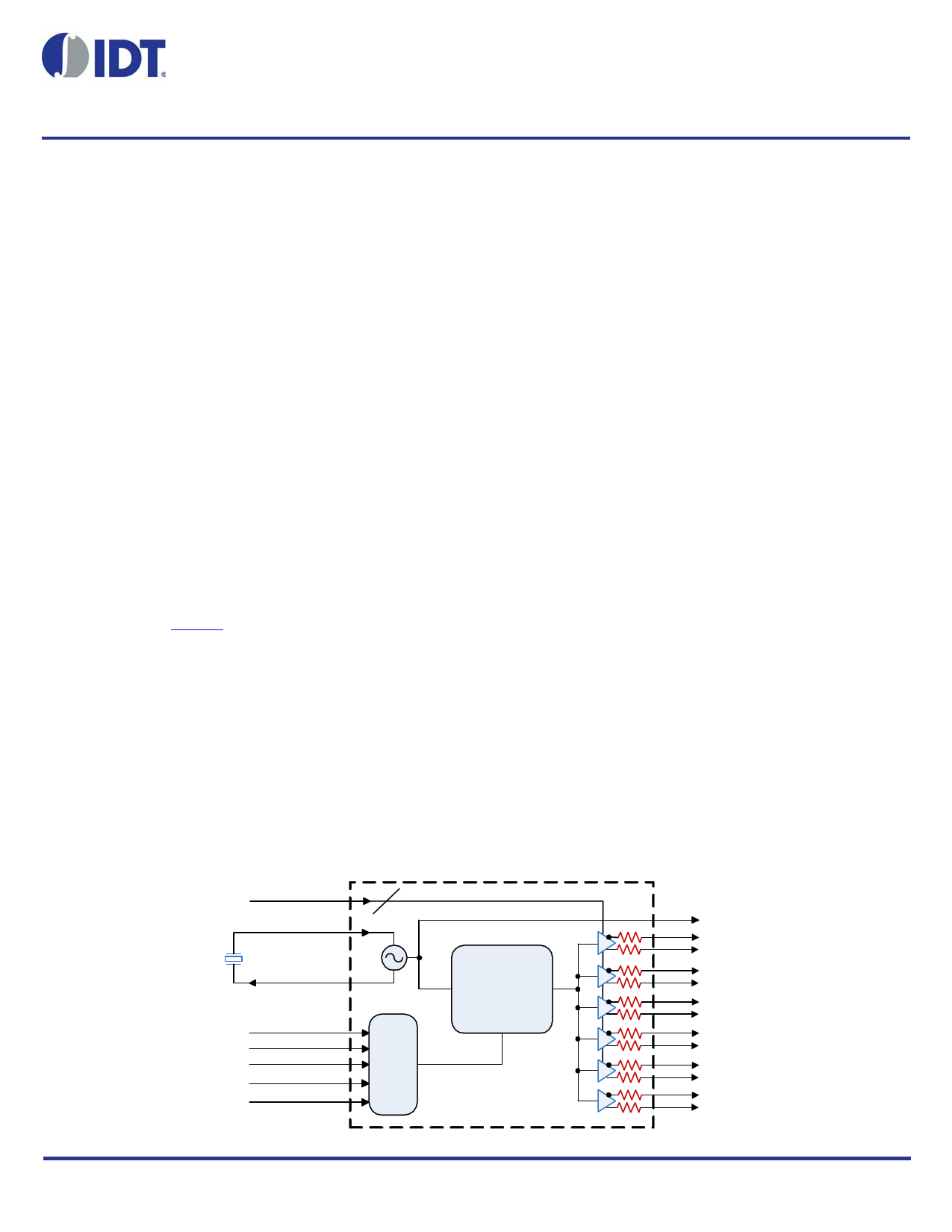
Block Diagram
Features/Benefits
• Direct connection to 100 (xx41) or 85 (xx51)
transmission lines; saves 24 resistors compared to
standard PCIe devices
• 172mW typical power consumption (@3.3V); eliminates
thermal concerns
• SMBus-selectable features allows optimization to customer
requirements:
• control input polarity
• control input pull up/downs
• slew rate for each output
• differential output amplitude
• 33, 85 or 100Ω output impedance for each output
• spread spectrum amount
• 41 and 51 devices contain default configuration; SMBus
interface not required for device operation
• P1 device allows factory programming of customer-defined
SMBus power up default; allows exact optimization to
customer requirements
• 8MHz - 40MHz input frequency with 9FGL08P1 device
(25MHz default); flexibility
• OE# pins; support DIF power management
• Pin/SMBus selectable 0%, -0.25% or -0.5% spread on DIF
outputs; minimize EMI and phase jitter for each application
• DIF outputs blocked until PLL is locked; clean system
start-up
• Two selectable SMBus addresses; multiple devices can
easily share an SMBus segment
• Space saving 40-pin 5x5mm VFQFPN; minimal board
space
vOE(5:0)#
XIN/CLKIN_25
603-25-150JA4I 25MHz
X2
6
vSADR
vSS_EN_tri
^CKPWRGD_PD#
SDATA_3.3
SCLK_3.3
Control
Logic
SSC Capable
PLL
REF
DIF5
DIF4
DIF3
DIF2
DIF1
DIF0
Note: Resistors default to internal on 41/51 devices. P1 devices have programmable default impedances on an output-by-output basis.
9FGL06 OCTOBER 19, 2016
1 ©2016 Integrated Device Technology, Inc.
1 page 
9FGL06 DATASHEET
Absolute Maximum Ratings
Stresses above the ratings listed below can cause permanent damage to the 9FGL06. These ratings, which are standard values
for IDT commercially rated parts, are stress ratings only. Functional operation of the device at these or any other conditions
above those indicated in the operational sections of the specifications is not implied. Exposure to absolute maximum rating
conditions for extended periods can affect product reliability. Electrical parameters are guaranteed only over the recommended
operating temperature range.
PARAMETER
SYMBOL
CONDITIONS
3.3V Supply Voltage
VDDxx Applies to VDD, VDDA and VDDIO, if present.
Input Voltage
VIN
Input High Voltage, SMBus VIHSMB
SMBus clock and data pins
Storage Temperature
Ts
Junction Temperature
Tj
Input ESD protection ESD prot
Human Body Model
1Guaranteed by design and characterization, not 100% tested in production.
2 Operation under these conditions is neither implied nor guaranteed.
3 Not to exceed 4.5V.
MIN
-0.5
-0.5
-65
2500
Electrical Characteristics–SMBus Parameters
TA = TAMB; Supply Voltages per normal operation conditions, See Test Loads for Loading Conditions
PARAMETER
SYMBOL
CONDITIONS
MIN
SMBus Input Low Voltage VILSMB
VDDSMB = 3.3V
SMBus Input High Voltage VIHSMB
VDDSMB = 3.3V
SMBus Output Low Voltage VOLSMB
@ IPULLUP
SMBus Sink Current
IPULLUP
@ VOL
Nominal Bus Voltage
VDDSMB
SCLK/SDATA Rise Time
tRSMB
(Max VIL - 0.15) to (Min VIH + 0.15)
SCLK/SDATA Fall Time
tFSMB
(Min VIH + 0.15) to (Max VIL - 0.15)
SMBus Operating
Frequency
fSMB
SMBus operating frequency
1 Guaranteed by design and characterization, not 100% tested in production.
2. The device must be powered up for the SMBus to function.
2.1
4
2.7
TYP MAX UNITS NOTES
3.9 V 1,2
VDD + 0.5V V
1, 3
3.9 V 1
150 °C 1
125 °C 1
V1
TYP MAX UNITS NOTES
0.8 V
3.6 V
0.4 V
mA
3.6 V
1000 ns 1
300 ns 1
500 kHz 2
OCTOBER 19, 2016
5 6-OUTPUT 3.3V PCIE CLOCK GENERATOR
5 Page 
9FGL06 DATASHEET
SMBus Table: Output Enable Register 1
Byte 0
Name
Control Function
Type
0
1 Default
Bit 7
Bit 6
DIF OE5
DIF OE4
Output Enable
Output Enable
RW
RW
See B11[1:0]
Pin controlled
Pin controlled
1
1
Bit 5
Reserved
X
Bit 4
DIF OE3
Output Enable
RW
Pin controlled
1
Bit 3
DIF OE2
Output Enable
RW See B11[1:0]
Pin controlled
1
Bit 2
DIF OE1
Output Enable
RW
Pin controlled
1
Bit 1
Reserved
X
Bit 0
DIF OE0
Output Enable
RW See B11[1:0]
Pin controlled
1
1. A low on these bits will overide the OE# pin and force the differential output to the state indicated by B11[1:0] (Low/Low default)
SMBus Table: SS Readback and Control Register
Byte 1
Name
Control Function
Bit 7
SSENRB1
SS Enable Readback Bit1
Bit 6
SSENRB1
SS Enable Readback Bit0
Type
0
1 Default
R 00' for SS_EN_tri = 0, '01' for SS_EN_tri Latch
R = 'M', '11 for SS_EN_tri = '1' Latch
Bit 5
SSEN_SWCNTRL
Enable SW control of SS
RW
SS control locked
Values in B1[4:3]
control SS amount.
0
Bit 4
SSENSW1
SS Enable Software Ctl Bit1 RW1
Bit 3
SSENSW0
SS Enable Software Ctl Bit0 RW1
Bit 2
Reserved
Bit 1
Bit 0
AMPLITUDE 1
AMPLITUDE 0
Controls Output Amplitude
RW
RW
1. B1[5] must be set to a 1 for these bits to have any effect on the part.
00' = SS Off, '01' = -0.25% SS,
'10' = Reserved, '11'= -0.5% SS
00 = 0.6V
10 = 0.75V
01= 0.68V
11 = 0.85V
0
0
X
1
0
SMBus Table: DIF Slew Rate Control Register
Byte 2
Name
Control Function
Bit 7
SLEWRATESEL DIF5
Adjust slew rate of DIF5
Bit 6
SLEWRATESEL DIF4
Adjust slew rate of DIF4
Bit 5
Reserved
Bit 4
SLEWRATESEL DIF3
Adjust slew rate of DIF3
Bit 3
SLEWRATESEL DIF2
Adjust slew rate of DIF2
Bit 2
SLEWRATESEL DIF1
Adjust slew rate of DIF1
Bit 1
Reserved
Bit 0
SLEWRATESEL DIF0
Adjust slew rate of DIF0
Note: See "Low-Power HCSL Outputs" table for slew rates.
Type
RW
RW
RW
RW
RW
RW
0
Slow Setting
Slow Setting
Slow Setting
Slow Setting
Slow Setting
Slow Setting
1
Fast Setting
Fast Setting
Fast Setting
Fast Setting
Fast Setting
Fast Setting
Default
1
1
X
1
1
1
X
1
SMBus Table: Nominal Vhigh Amplitude Control/ REF Control Register
Byte 3
Name
Control Function
Type
0
Bit 7
Bit 6
REF
Slew Rate Control
RW 00 = Slowest
RW 10 = Fast
Bit 5 REF Power Down Function Wake-on-Lan Enable for REF RW
REF disabled in
Power Down
Bit 4
REF OE
REF Output Enable
RW Disabled1
Bit 3
Reserved
Bit 2
Bit 1
Reserved
Reserved
Bit 0
Reserved
1. The disabled state depends on Byte11[1:0]. '00' = Low, '01'=HiZ, '10'=Low, '11'=HIgh
1
01 =Slow
11 = Fastest
REF runs in Power
Down
Enabled
Default
0
1
0
1
X
X
X
X
Byte 4 is Reserved
OCTOBER 19, 2016
11 6-OUTPUT 3.3V PCIE CLOCK GENERATOR
11 Page | ||
| Páginas | Total 19 Páginas | |
| PDF Descargar | [ Datasheet 9FGL06.PDF ] | |
Hoja de datos destacado
| Número de pieza | Descripción | Fabricantes |
| 9FGL02 | 2-output 3.3V PCIe Clock Generator | IDT |
| 9FGL04 | 4-output 3.3V PCIe Clock Generator | IDT |
| 9FGL06 | 6-output 3.3V PCIe Clock Generator | IDT |
| 9FGL08 | 8-output 3.3V PCIe Clock Generator | IDT |
| Número de pieza | Descripción | Fabricantes |
| SLA6805M | High Voltage 3 phase Motor Driver IC. |
Sanken |
| SDC1742 | 12- and 14-Bit Hybrid Synchro / Resolver-to-Digital Converters. |
Analog Devices |
|
DataSheet.es es una pagina web que funciona como un repositorio de manuales o hoja de datos de muchos de los productos más populares, |
| DataSheet.es | 2020 | Privacy Policy | Contacto | Buscar |