|
|
|
PDF 8V79S674 Data sheet ( Hoja de datos )
| Número de pieza | 8V79S674 | |
| Descripción | LVPECL Clock Divider and Fanout Buffer | |
| Fabricantes | IDT | |
| Logotipo | ||
Hay una vista previa y un enlace de descarga de 8V79S674 (archivo pdf) en la parte inferior de esta página. Total 21 Páginas | ||
|
No Preview Available !
Differential-to-3.3V, 2.5V LVPECL
Clock Divider and Fanout Buffer
8V79S674
DATA SHEET
General Description
The 8V79S674 is a clock divider and fanout buffer. The device has
been designed for clock signal division in wireless base station radio
equipment boards. The device is optimized to deliver excellent
additive phase jitter performance. The 8V79S674 uses SiGe
technology for an optimum of high clock frequency and low phase
noise performance, combined with high power supply noise rejection.
The device offers the frequency division by ÷1, ÷2, ÷4 and ÷8. Four
low-skew LVPECL outputs are available and support clock output
frequencies up to 2500MHz (÷1 frequency division). Outputs can be
disabled to save power consumption if not used. The device is
packaged in a lead-free (RoHS 6) 20-lead VFQFN package. The
extended temperature range supports wireless infrastructure,
telecommunication and networking end equipment requirements.
Features
• Clock signal division and distribution
• SiGe technology for high-frequency and fast signal rise/fall times
• Four low-skew LVPECL clock outputs
• Supports frequency division of ÷1, ÷2, ÷4 and ÷8
• Maximum frequency: 2500MHz
• Maximum output skew: 50ps (maximum)
• Maximum LVPECL output rise/fall time: 200ps (maximum)
• 3.3V or 2.5V core and output supply mode
• Supports 1.8V I/O logic levels for all control pins
• -40°C to 85°C ambient operating temperature
• Available in lead-free (RoHS 6) package
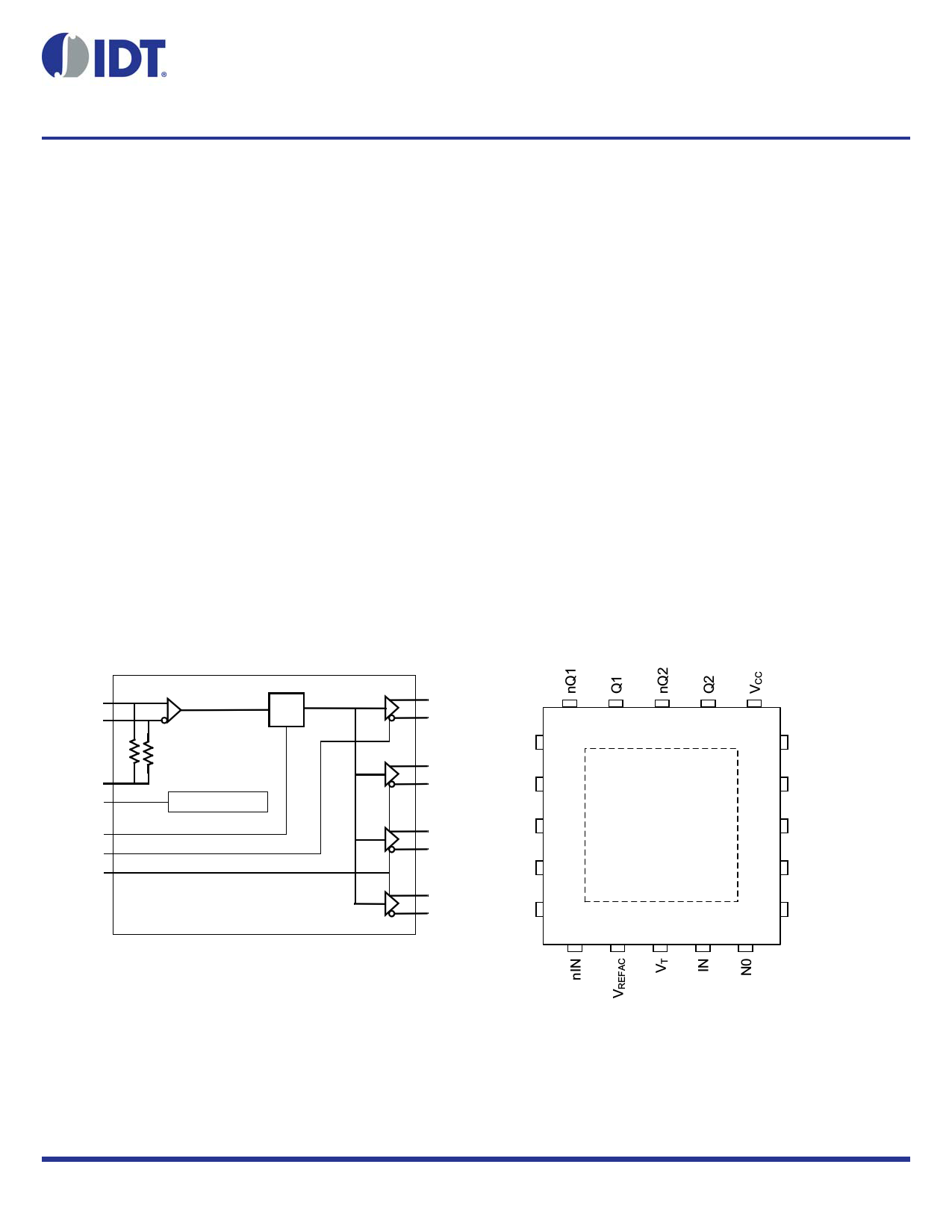
Block Diagram
IN ÷N
nIN
2x 50
VT
VREFAC
Reference Voltage
N[1:0]
nOEA
nOEB
Pulldown
Pulldown
Pulldown
.
8V79S674 REVISION 2 04/10/15
Pin Assignment
Q0
nQ0
Q1
nQ1
15 14 13 12 11
VCC 16
10 Q3
Q0 17
9 nQ3
Q2
nQ2
Q3
nQ3
nQ0 18
nOEA 19
VEE 20
1
8V79S674
8 nOEB
7 N1
6 VEE
2 3 45
20-pin, 4mm x 4mm VFQFN Package
1 ©2015 Integrated Device Technology, Inc.
1 page 
8V79S674 DATA SHEET
Table 4D. Differential DC Characteristics, VCC = 3.3V ± 5% or 2.5V ± 5%, VEE = 0V, TA = -40°C to 85°C
Symbol
Parameter
Test Conditions
Minimum
Typical
Maximum
RIN
Input
Resistance
IN, nIN
IN to VT, nIN to VT
40 50 60
IIN
VREFAC
Input Current IN, nIN
Bias Voltage
VCC = 2.5V or 3.3V
IREFAC = ± 1mA
VCC – 1.5
VCC – 1.28
30
VCC – 1.0
Units
mA
V
Table 4E. LVPECL DC Characteristics, VCC = 3.3V ± 5%, VEE = 0V, TA = -40°C to 85°C
Symbol
Parameter
Test Conditions
Minimum
VOH Output High Voltage1
VCC – 1.1
VOL Output Low Voltage; NOTE 1
VCC – 1.8
VOUT
Output Voltage Swing
0.5
VDIFF_OUT
Differential Output Voltage
Swing
1
NOTE 1. Outputs terminated with 50 to VCC – 2V.
Typical
Maximum
VCC – 0.7
VCC – 1.4
1
2
Units
V
V
V
V
Table 4F. LVPECL DC Characteristics, VCC = 2.5V ± 5%, VEE = 0V, TA = -40°C to 85°C
Symbol
Parameter
Test Conditions
Minimum
VOH Output High Voltage1
VOL Output Low Voltage1
VCC – 1.1
VCC – 1.8
VOUT
Output Voltage Swing
0.5
VDIFF_OUT
Differential Output Voltage
Swing
1
NOTE 1. Outputs terminated with 50 to VCC – 2V.
Typical
Maximum
VCC – 0.7
VCC – 1.4
1.0
2
Units
V
V
V
V
REVISION 2 04/10/15
5 DIFFERENTIAL-TO-3.3V, 2.5V LVPECL
CLOCK DIVIDER AND FANOUT BUFFER
5 Page 
8V79S674 DATA SHEET
3.3V LVPECL Input with Built-In 50 Termination Interface
The IN /nIN with built-in 50 terminations accept LVDS, LVPECL,
CML and other differential signals. Both VOH and VOL must meet the
VIN and VIH input requirements. Figures 2A to 2D show interface
examples for the IN /nIN input with built-in 50 terminations driven by
the most common driver types. The input interfaces suggested here
are examples only. If the driver is from another vendor, use their
termination recommendation. Please consult with the vendor of the
driver component to confirm the driver termination requirements.
Figure 2A. IN/nIN Input with Built-In 50
Driven by an LVDS Driver
Figure 2B. IN/nIN Input with Built-In 50
Driven by an LVPECL Driver
3.3V
3.3V CML with
Built-In Pullup
Zo = 50Ω
C1
Zo = 50Ω
C2
3.3V
IN
50Ω
VT
50Ω
nIN
V_REF_AC
Receiver with
Built-In 50Ω
Figure 2C. IN/nIN Input with Built-In 50
Driven by a CML Driver with Open Collector
Figure 2D. IN/nIN Input with Built-In 50
Driven by a CML Driver with Built-In 50
Pullup
REVISION 2 04/10/15
11 DIFFERENTIAL-TO-3.3V, 2.5V LVPECL
CLOCK DIVIDER AND FANOUT BUFFER
11 Page | ||
| Páginas | Total 21 Páginas | |
| PDF Descargar | [ Datasheet 8V79S674.PDF ] | |
Hoja de datos destacado
| Número de pieza | Descripción | Fabricantes |
| 8V79S674 | LVPECL Clock Divider and Fanout Buffer | IDT |
| Número de pieza | Descripción | Fabricantes |
| SLA6805M | High Voltage 3 phase Motor Driver IC. |
Sanken |
| SDC1742 | 12- and 14-Bit Hybrid Synchro / Resolver-to-Digital Converters. |
Analog Devices |
|
DataSheet.es es una pagina web que funciona como un repositorio de manuales o hoja de datos de muchos de los productos más populares, |
| DataSheet.es | 2020 | Privacy Policy | Contacto | Buscar |