|
|
|
PDF IDT8SLVP1104I Data sheet ( Hoja de datos )
| Número de pieza | IDT8SLVP1104I | |
| Descripción | LVPECL Output Fanout Buffer | |
| Fabricantes | IDT | |
| Logotipo | ||
Hay una vista previa y un enlace de descarga de IDT8SLVP1104I (archivo pdf) en la parte inferior de esta página. Total 22 Páginas | ||
|
No Preview Available !
Low Phase Noise,1-to-4, 3.3V, 2.5V
LVPECL Output Fanout Buffer
IDT8SLVP1104I
DATASHEET
General Description
The IDT8SLVP1104I is a high-performance differential LVPECL
fanout buffer. The device is designed for the fanout of high-frequency,
very low additive phase-noise clock and data signals. The
IDT8SLVP1104I is characterized to operate from a 3.3V or 2.5V
power supply. Guaranteed output-to-output and part-to-part skew
characteristics make the IDT8SLVP1104I ideal for those clock
distribution applications demanding well-defined performance and
repeatability.Four low skew outputs are available. The integrated bias
voltage reference enables easy interfacing of single-ended signals to
the device inputs. The device is optimized for low power consumption
and low additive phase noise.
Features
• Four low skew, low additive jitter LVPECL differential output pairs
• Differential LVPECL input pair can accept the following differential
input levels: LVDS, LVPECL, CML
• Differential PCLKx pairs can also accept single-ended LVCMOS
levels. See the Applications section Writing the Differential Input
Levels to Accept Single-ended Levels (Figures 1 and 2)
• Maximum input clock frequency: 2GHz
• LVCMOS interface levels for the control input (input select)
• Output skew: 5ps (typical)
• Propagation delay: 320ps (maximum)
• Low additive phase jitter, RMS; fREF = 156.25MHz, VPP = 1V,
12kHz - 20MHz: 40fs (maximum)
• Maximum device current consumption (IEE): 60mA (maximum)
• Full 3.3V or 2.5V supply voltage
• Lead-free (RoHS 6) packaging
• -40°C to 85°C ambient operating temperature
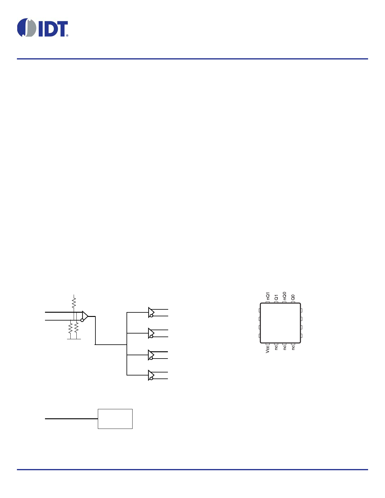
Block Diagram
VCC
PCLK Pulldown
nPCLK Pullup/Pulldown
fREF
VREF
Voltage
Reference
Pin Assignment
Q0
nQ0
Q1
nQ1
12 11 10 9
Q2 13
8 VREF
nQ2 14
7 nPCLK
Q3 15
6 PCLK
nQ3 16
5 VCC
1 23 4
Q2
nQ2
IDT8SLVP1104I
Q3 16 lead VFQFN
nQ3
3.0mm x 3.0mm x 0.925mm package body
1.7mm x 1.7mm Epad Size
NL Package
Top View
IDT8SLVP1104ANLGI REVISION A FEBRUARY 25, 2014
1
©2014 Integrated Device Technology, Inc.
1 page 
IDT8SLVP1104I Data Sheet
LOW PHASE NOISE, 1:4, 3.3V, 2.5V LVPECL OUTPUT FANOUT BUFFER
AC Electrical Characteristics
Table 4. AC Electrical Characteristics, VCC = 3.3V ± 5% or 2.5V ± 5%, VEE = 0V, TA = -40°C to 85°C
Symbol Parameter
Test Conditions
Minimum Typical
fREF
Input
PCLK,
Frequency nPCLK
V/t
Input
PCLK,
Edge Rate nPCLK
1.5
tPD
tsk(o)
Propagation Delay;
NOTE 1
Output Skew;
NOTE 2, 3
PCK, nPCLK to any Q[0:3], nQ[0:3]
for VPP = 0.1V or 0.3V
120 200
5
tsk(p)
tsk(pp)
Pulse Skew
Part-to-Part Skew;
NOTE 3, 4
fREF = 100MHz
5
100
fREF = 122.88MHz Sine Wave, VPP = 1V,
Integration Range: 1kHz – 40MHz
170
fREF = 122.88MHz Sine Wave, VPP = 1V,
Integration Range: 10kHz – 20MHz
114
fREF = 122.88MHz Sine Wave, VPP = 1V,
Integration Range: 12kHz – 20MHz
114
Buffer Additive Phase
fREF = 156.25MHz Square Wave, VPP = 1V,
Integration Range: 1kHz – 40MHz
tJIT
Jitter, RMS; refer to
Additive Phase Jitter
fREF = 156.25MHz Square Wave, VPP = 1V,
Integration Range: 10kHz – 20MHz
Section
fREF = 156.25MHz Square Wave, VPP = 1V,
Integration Range: 12kHz – 20MHz
42
32
32
fREF = 156.25MHz Square Wave, VPP = 0.5V,
Integration Range: 1kHz – 40MHz
51
fREF = 156.25MHz Square Wave, VPP = 0.5V,
Integration Range: 10kHz – 20MHz
38
fREF = 156.25MHz Square Wave, VPP = 0.5V,
Integration Range: 12kHz – 20MHz
38
tR / tF
VPP
VCMR
Output Rise/ Fall Time
Peak-to-Peak Input
Voltage; NOTE 5, 6
Common Mode Input
Voltage; NOTE 5, 6, 7
20% to 80%
fREF < 1.5 GHz
fREF > 1.5 GHz
35
0.1
0.2
1.0
VO(pp)
VDIFF_OUT
Output Voltage Swing,
Peak-to-Peak
Differential Output
Voltage Swing,
Peak-to-Peak
VCC = 3.3V, fREF 2GHz
VCC = 2.5V, fREF 2GHz
VCC = 3.3V, fREF 2GHz
VCC = 2.5V, fREF 2GHz
0.45 0.75
0.4 0.65
0.9 1.5
0.8 1.3
Maximum Units
2 GHz
V/ns
320 ps
25 ps
20 ps
200 ps
fs
fs
fs
51 fs
40 fs
40 fs
71 fs
52 fs
52
180
1.5
1.5
VCC – 0.6
1.0
1.0
2.0
2.0
fs
ps
V
V
V
V
V
V
V
NOTE: Electrical parameters are guaranteed over the specified ambient operating temperature range, which is established when the device is
mounted in a test socket with maintained transverse airflow greater than 500 lfpm. The device will meet specifications after thermal equilibrium
has been reached under these conditions.
NOTE 1: Measured from the differential input crossing point to the differential output crossing point.
NOTE 2: Defined as skew between outputs at the same supply voltage and with equal load conditions. Measured at the differential crosspoints.
NOTE 3: This parameter is defined in accordance with JEDEC Standard 65.
NOTES continued on next page.
IDT8SLVP1104ANLGI REVISION A FEBRUARY 25, 2014
5
©2014 Integrated Device Technology, Inc.
5 Page 
IDT8SLVP1104I Data Sheet
LOW PHASE NOISE, 1:4, 3.3V, 2.5V LVPECL OUTPUT FANOUT BUFFER
3.3V LVPECL Clock Input Interface
The PCLK /nPCLK accepts LVPECL, LVDS, CML and other
differential signals. Both signals must meet the VPP and VCMR input
requirements. Figures 2A to 2E show interface examples for the
PCLK/ nPCLK input driven by the most common driver types. The
input interfaces suggested here are examples only. If the driver is
from another vendor, use their termination recommendation. Please
consult with the vendor of the driver component to confirm the driver
termination requirements.
3.3V
CML
3.3V
3.3V
PCLK
nPCLK
LVPECL
Input
3.3V
Zo = 50Ω
CML Built-In Pullup
Zo = 50Ω
R1
100Ω
3.3V
PCLK
nPCLK
LVPECL
Input
Figure 2A. PCLK/nPCLK Input Driven by a CML Driver
Figure 2B. PCLK/nPCLK Input Driven by a
Built-In Pullup CML Driver
3.3V
LVPECL
Zo = 50Ω
Zo = 50Ω
3.3V
R3
125Ω
R4
125Ω
3.3V
PCLK
nPCLK
LVPECL
R1 R2
84Ω 84Ω
Input
Figure 2C. PCLK/nPCLK Input Driven by a
3.3V LVPECL Driver
Figure 2D. PCLK/nPCLK Input Driven by a
3.3V LVPECL Driver with AC Couple
3.3V
LVDS
Zo = 50
Zo = 50
3.3V
R1
100
PCLK
nPCLK
LVPECL
Input
Figure 2E. PCLK/nPCLK Input Driven by a
3.3V LVDS Driver
IDT8SLVP1104ANLGI REVISION A FEBRUARY 25, 2014
11
©2014 Integrated Device Technology, Inc.
11 Page | ||
| Páginas | Total 22 Páginas | |
| PDF Descargar | [ Datasheet IDT8SLVP1104I.PDF ] | |
Hoja de datos destacado
| Número de pieza | Descripción | Fabricantes |
| IDT8SLVP1104I | LVPECL Output Fanout Buffer | IDT |
| Número de pieza | Descripción | Fabricantes |
| SLA6805M | High Voltage 3 phase Motor Driver IC. |
Sanken |
| SDC1742 | 12- and 14-Bit Hybrid Synchro / Resolver-to-Digital Converters. |
Analog Devices |
|
DataSheet.es es una pagina web que funciona como un repositorio de manuales o hoja de datos de muchos de los productos más populares, |
| DataSheet.es | 2020 | Privacy Policy | Contacto | Buscar |