|
|
|
PDF ICS8S89834I Data sheet ( Hoja de datos )
| Número de pieza | ICS8S89834I | |
| Descripción | 2-to-4 LVCMOS/LVTTL-toLVPECL/ECL Clock Multiplexer | |
| Fabricantes | IDT | |
| Logotipo | ||
Hay una vista previa y un enlace de descarga de ICS8S89834I (archivo pdf) en la parte inferior de esta página. Total 17 Páginas | ||
|
No Preview Available !
Low Skew, 2-to-4 LVCMOS/LVTTL-to-
LVPECL/ECL Clock Multiplexer
ICS8S89834I
DATA SHEET
General Description
The ICS8S89834I is a high speed 2-to-4
ICS LVCMOS/LVTTL-to-LVPECL/ECL Clock Multiplexer.
HiPerClockS™ The ICS8S89834I is optimized for high speed and very
low output skew, making it suitable for use in
demanding applications such as SONET, 1 Gigabit
and 10 Gigabit Ethernet, and Fibre Channel. The device also has an
output enable pin which may be useful for system test and debug
purposes. The ICS8S89834I is packaged in a small 3mm x 3mm
16-pin VFQFN package which makes it ideal for use in
space-constrained applications.
Features
• Four differential LVPECL/ECL output pairs
• Two LVCMOS/LVTTL clock inputs
• Maximum output frequency: 1GHz
• Output skew: 30ps (maximum)
• Part-to-part skew: 100ps (maximum)
• Propagation delay: 550ps (maximum)
• Additive phase jitter, RMS: 0.12ps (typical)
• Full 3.3V and 2.5V operating supply modes
• -40°C to 85°C ambient operating temperature
• Available in lead-free (RoHS 6) package
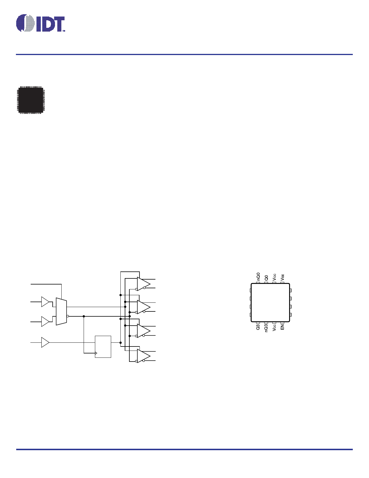
Block Diagram
SEL Pullup
IN1 Pullup
IN2 Pullup
1
0
EN Pullup
DQ
CK
Q0
nQ0
Q1
nQ1
Q2
nQ2
Q3
nQ3
Pin Assignment
16 15 14 13
Q1 1
12 IN1
nQ1 2
11 SEL
Q2 3
10 nc
nQ2 4
9 IN2
5 6 78
ICS8S89834I
16-Lead VFQFN
3mm x 3mm x 0.925mm package body
K Package
Top View
ICS8S89834AKI REVISION A FEBRUARY 4, 2010
1
©2010 Integrated Device Technology, Inc.
1 page 
ICS8S89834I Data Sheet
LOW SKEW, 2-TO-4 LVCMOS/LVTTL-TO-LVPECL/ECL CLOCK MULTIPLEXER
Table 4D. LVPECL DC Characteristics, VCC = 3.3V ± 10% or 2.5V ± 5%, VEE = 0V, TA = -40°C to 85°C
Symbol Parameter
Test Conditions
Minimum
Typical
Maximum
VOH Output High Voltage; NOTE 1
VOL Output Low Voltage; NOTE 1
VOUT
Output Voltage Swing
VDIFF_OUT Differential Output Voltage Swing
VCC – 1.145
VCC – 1.945
0.6
1.2
VCC – 0.80
VCC – 1.60
1.0
2.0
NOTE 1: Outputs terminated with 50Ω to VCC - 2V.
Units
V
V
V
V
AC Electrical Characteristics
Table 5. AC Characteristics, VCC = 2.5V ± 5% or or 3.3V ± 10%, TA = -40°C to 85°C
Symbol Parameter
Test Conditions
Minimum
fMAX
tPLH
tPHL
tSW
tsk(o)
Maximum Frequency
Propagation Delay; Low-to-High; NOTE 1
Propagation Delay; High-to-Low; NOTE 1
Switchover Time
SEL to Q
Output Skew; NOTE 2, 3
250
300
300
tsk(pp) Part-to-Part Skew; NOTE 3, 4
tjit
Buffer Additive Phase Jitter, RMS; refer to
Additive Phase Jitter Section
200MHz
Integration Range:
(12kHz - 20MHz)
tS
tH
tR / tF
odc
Clock Enable Setup Time
Clock Enable Hold Time
Output Rise/Fall Time
EN to IN1, IN2
EN to IN1, IN2
Output Duty Cycle
20% to 80%
fMAX < 622MHz
fMAX ≥ 622MHz
300
500
50
48
45
Typical
0.12
Maximum
1
550
550
550
30
100
250
52
55
Units
GHz
ps
ps
ps
ps
ps
ps
ps
ps
ps
%
%
NOTE: Electrical parameters are guaranteed over the specified ambient operating temperature range, which is established when the device
is mounted in a test socket with maintained transverse airflow greater than 500 lfpm. The device will meet specifications after thermal
equilibrium has been reached under these conditions.
All parameters are measured at ≤ 1GHz unless otherwise noted.
NOTE 1: Measured from VCC/2 of the input to the differential output crossing point.
NOTE 2: Defined as skew between outputs at the same supply voltage and with equal load conditions.
Measured at the output differential cross points.
NOTE 3: This parameter is defined in accordance with JEDEC Standard 65.
NOTE 4: Defined as skew between outputs on different devices operating at the same supply voltage, same frequency and with equal load
conditions. Using the same type of inputs on each device, the outputs are measured at the differential cross points.
ICS8S89834AKI REVISION A FEBRUARY 4, 2010
5
©2010 Integrated Device Technology, Inc.
5 Page 
ICS8S89834I Data Sheet
LOW SKEW, 2-TO-4 LVCMOS/LVTTL-TO-LVPECL/ECL CLOCK MULTIPLEXER
Termination for 2.5V LVPECL Outputs
Figure 4A and Figure 4B show examples of termination for 2.5V
LVPECL driver. These terminations are equivalent to terminating 50Ω
to VCC – 2V. For VCC = 2.5V, the VCC – 2V is very close to ground
level. The R3 in Figure 4B can be eliminated and the termination is
shown in Figure 4C.
VCC = 2.5V
50Ω
50Ω
2.5V LVPECL Driver
2.5V
R1 R3
250 250
2.5V
+
–
R2 R4
62.5 62.5
VCC = 2.5V
50Ω
50Ω
2.5V LVPECL Driver
2.5V
+
–
R1 R2
50 50
R3
18
Figure 4A. 2.5V LVPECL Driver Termination Example
Figure 4B. 2.5V LVPECL Driver Termination Example
VCC = 2.5V
50Ω
50Ω
2.5V LVPECL Driver
2.5V
+
–
R1 R2
50 50
Figure 4C. 2.5V LVPECL Driver Termination Example
ICS8S89834AKI REVISION A FEBRUARY 4, 2010
11
©2010 Integrated Device Technology, Inc.
11 Page | ||
| Páginas | Total 17 Páginas | |
| PDF Descargar | [ Datasheet ICS8S89834I.PDF ] | |
Hoja de datos destacado
| Número de pieza | Descripción | Fabricantes |
| ICS8S89834I | 2-to-4 LVCMOS/LVTTL-toLVPECL/ECL Clock Multiplexer | IDT |
| Número de pieza | Descripción | Fabricantes |
| SLA6805M | High Voltage 3 phase Motor Driver IC. |
Sanken |
| SDC1742 | 12- and 14-Bit Hybrid Synchro / Resolver-to-Digital Converters. |
Analog Devices |
|
DataSheet.es es una pagina web que funciona como un repositorio de manuales o hoja de datos de muchos de los productos más populares, |
| DataSheet.es | 2020 | Privacy Policy | Contacto | Buscar |