|
|
|
PDF 8P34S2104 Data sheet ( Hoja de datos )
| Número de pieza | 8P34S2104 | |
| Descripción | Dual 1:4 LVDS Output 1.8V Fanout Buffer | |
| Fabricantes | IDT | |
| Logotipo | ||
Hay una vista previa y un enlace de descarga de 8P34S2104 (archivo pdf) en la parte inferior de esta página. Total 19 Páginas | ||
|
No Preview Available !
Dual 1:4 LVDS Output 1.8V Fanout Buffer
8P34S2104
Datasheet
Description
The 8P34S2104 is a high-performance, low-power, differential
dual 1:4 LVDS Output 1.8V fanout buffer. The device is designed
for the fanout of high-frequency, very low additive phase-noise
clock and data signals. Two independent buffer channels are
available. Each channel has four low-skew outputs. High isolation
between channels minimizes noise coupling. AC characteristics
such as propagation delay are matched between channels.
Guaranteed output-to-output and part-to-part skew characteristics
make the 8P34S2104 ideal for those clock distribution
applications demanding well-defined performance and
repeatability. The device is characterized to operate from a 1.8V
power supply. The integrated bias voltage references enable easy
interfacing of AC-coupled signals to the device inputs.
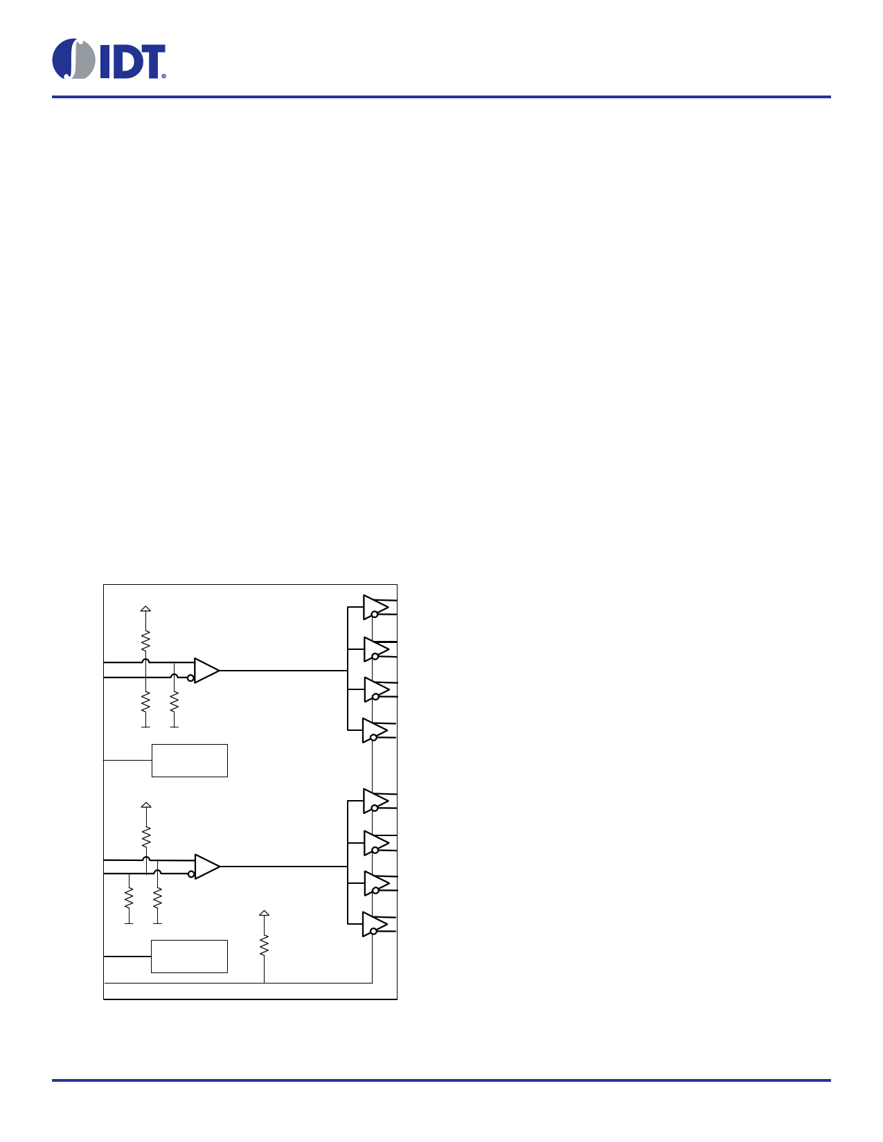
Block Diagram
Features
▪ Dual 1:4 low skew, low additive jitter LVDS fanout buffers
▪ Matched AC characteristics across both channels
▪ High isolation between channels
▪ Low power consumption
▪ Both differential CLKA, nCLKA and CLKB, nCLKB inputs
accept LVDS, LVPECL and single-ended LVCMOS levels
▪ Maximum input clock frequency: 2GHz
▪ Output amplitudes: 350mV, 500mV (selectable)
▪ Output bank skew: 8ps typical
▪ Output skew: 10ps typical
▪ Low additive phase jitter, RMS: 45fs typical
(fREF = 156.25MHz, 12kHz - 20MHz)
▪ Full 1.8V supply voltage mode
▪ Device current consumption (IDD): 135mA typical
▪ Lead-free (RoHS 6), 28-lead VFQFN packaging
▪ -40°C to 85°C ambient operating temperature
▪ Supports case temperature up to 105°C
CLKA
nCLKA
VDDQA
51k
51k 51k
VREFA
Voltage
Reference A
VDDQB
CLKB
nCLKB
51k
51k 51k
VDDQB
VREFB
SELA
Voltage
Reference B
8P34S2104 transistor count:
51k
QA0
nQA0
QA1
nQA1
QA2
nQA2
QA3
nQA3
QB0
nQB0
QB1
nQB1
QB2
nQB2
QB3
nQB3
©2016 Integrated Device Technology, Inc.
1
October 20, 2016
1 page 
8P34S2104 Datasheet
Table 6. LVCMOS Inputs DC Characteristics, VDDQA = VDDQB = 1.8V ± 5%, TA = -40°C to 85°C
Symbol
Parameter
VIH Input high voltage SELA
VIL Input low voltage SELA
IIH Input high current SELA
IIL Input low current SELA
Test Conditions
VIN = VDD[a] = 1.89V
VIN = 0V, VDD[a] = 1.89V
Minimum
0.65 · VDD[a]
-0.3
-150
Typical
Maximum
VDD[a] + 0.3
0.35 · VDD[a]
10
Units
V
V
µA
µA
[a] VDD denotes VDDA, VDDB.
Table 7. Differential Inputs Characteristics, VDDQA = VDDQB = 1.8V ± 5%, TA = -40°C to 85°C
Symbol
Parameter
IIH Input high current CLKA, nCLKA
CLKB, nCLKB
IIL
VREF
Input low current
CLKA, CLKB
nCLKA, nCLKB
Reference voltage[b]
Test Conditions
VIN = VDD[a] = 1.89V
VIN = 0V, VDD[a] = 1.89V
VIN = 0V, VDD[a] = 1.89V
IREF = +100µA, VDD[a] = 1.8V
Minimum
-10
-150
0.9
Typical
Maximum
150
1.30
[a] VDD denotes VDDA, VDDB.
[b] VREF specification is applicable to the AC-coupled input interfaces shown in Figure 5 and Figure 6.
Units
µA
µA
µA
V
Table 8. LVDS DC Characteristics, VDDQA = VDDQB = 1.8V ± 5%, TA = -40°C to 85°C
Symbol
Parameter
Test Conditions
Minimum Typical
VOD
VOS
VOD Magnitude Change
VOS Magnitude Change
Maximum
50
50
Units
mV
mV
©2016 Integrated Device Technology, Inc.
5
October 20, 2016
5 Page 
8P34S2104 Datasheet
1.8V Differential Clock Input Interface
The CLK /nCLK accepts LVDS, LVPECL and other differential signals. The differential input signal must meet both the VPP and VCMR
input requirements. Figure 4 to Figure 6 show interface examples for the CLK /nCLK input driven by the most common driver types. The
input interfaces suggested here are examples only. If the driver is from another vendor, use their termination recommendation. Please
consult with the vendor of the driver component to confirm the driver termination requirements.
Figure 4. Differential Input Driven by an LVDS Driver - DC Coupling
Figure 5. Differential Input Driven by an LVDS Driver - AC Coupling
Figure 6. Differential Input Driven by an LVPECL Driver - AC Coupling
©2016 Integrated Device Technology, Inc.
11
October 20, 2016
11 Page | ||
| Páginas | Total 19 Páginas | |
| PDF Descargar | [ Datasheet 8P34S2104.PDF ] | |
Hoja de datos destacado
| Número de pieza | Descripción | Fabricantes |
| 8P34S2102 | Dual 1:2 LVDS Output 1.8V Fanout Buffer | IDT |
| 8P34S2104 | Dual 1:4 LVDS Output 1.8V Fanout Buffer | IDT |
| 8P34S2106 | Dual 1:6 LVDS Output 1.8V Fanout Buffer | IDT |
| 8P34S2108 | Dual 1:8 LVDS Output 1.8V Fanout Buffer | IDT |
| Número de pieza | Descripción | Fabricantes |
| SLA6805M | High Voltage 3 phase Motor Driver IC. |
Sanken |
| SDC1742 | 12- and 14-Bit Hybrid Synchro / Resolver-to-Digital Converters. |
Analog Devices |
|
DataSheet.es es una pagina web que funciona como un repositorio de manuales o hoja de datos de muchos de los productos más populares, |
| DataSheet.es | 2020 | Privacy Policy | Contacto | Buscar |