|
|
|
PDF CLC2008 Data sheet ( Hoja de datos )
| Número de pieza | CLC2008 | |
| Descripción | 75MHz Rail-to-Rail Amplifiers | |
| Fabricantes | Exar | |
| Logotipo | ||
Hay una vista previa y un enlace de descarga de CLC2008 (archivo pdf) en la parte inferior de esta página. Total 16 Páginas | ||
|
No Preview Available !
Data Sheet
Comlinear® CLC1008, CLC2008
0.5mA, Low Cost, 2.5 to 5.5V, 75MHz Rail-to-Rail Amplifiers
FEATURES
n 505μA supply current
n 75MHz bandwidth
n Input voltage range with 5V supply:
-0.3V to 3.8V
n Output voltage range with 5V supply:
0.07V to 4.86V
n 50V/μs slew rate
n 12nV/√Hz input voltage noise
n 15mA linear output current
n Fully specified at 2.7V and 5V supplies
n Replaces AD8031 in VS ≤ 5 applications
General Description
The COMLINEAR CLC1008 (single) and CLC2008 (dual) offer superior dynamic
performance with 75MHz small signal bandwidth and 50V/μs slew rate. These
amplifiers use only 505μA of supply current and are designed to operate
from a supply range of 2.5V to 5.5V (±1.25 to ±2.75).The combination of
low power, high output current drive, and rail-to-rail performance make the
CLC1008 and CLC2008 well suited for battery-powered communication/
computing systems.
The combination of low cost and high performance make the CLC1008 and
CLC2008 suitable for high volume applications in both consumer and industrial
applications such as wireless phones, scanners, and color copiers.
APPLICATIONS
n Portable/battery-powered applications
n Mobile communications, cell phones,
pagers
n ADC buffer
n Active filters
n Portable test instruments
n Signal conditioning
n Medical Equipment
n Portable medical instrumentation
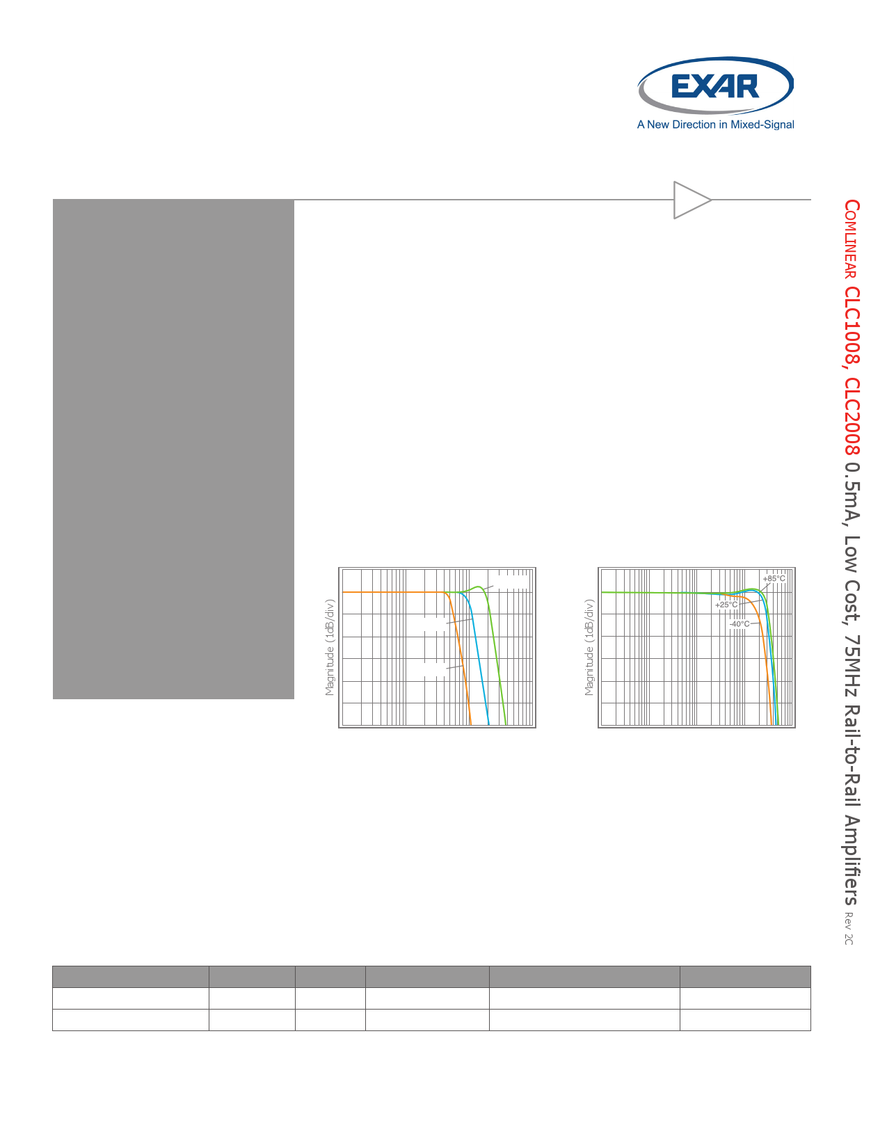
Typical Performance Examples
Frequency Response vs. VOUT
Vo = 1Vpp
Vo = 2Vpp
Vo = 4Vpp
Frequency Response vs. Temperature
0.1 1
10 100
Frequency (MHz)
0.01
0.1
1
10 100
Frequency (MHz)
Ordering Information
Part Number
Package
CLC1008IST5X
SOT23-5
CLC2008ISO8X
SOIC-8
Moisture sensitivity level for all parts is MSL-1.
Pb-Free
Yes
Yes
RoHS Compliant
Yes
Yes
Operating Temperature Range
-40°C to +85°C
-40°C to +85°C
Packaging Method
Reel
Reel
Exar Corporation
48720 Kato Road, Fremont CA 94538, USA
www.exar.com
Tel. +1 510 668-7000 - Fax. +1 510 668-7001
1 page 
Data Sheet
Electrical Characteristics at +5V
TA = 25°C, Vs = +5V, Rf = Rg =1kΩ, RL = 1kΩ to VS/2, G = 2; unless otherwise noted.
Symbol Parameter
Frequency Domain Response
UGBWSS
BWSS
BWLS
GBWP
Unity Gain -3dB Bandwidth
-3dB Bandwidth
Large Signal Bandwidth
Gain Bandwidth Product
Time Domain Response
tR, tF
tS
OS
Rise and Fall Time
Settling Time to 0.1%
Overshoot
SR Slew Rate
Distortion/Noise Response
HD2 2nd Harmonic Distortion
HD3 3rd Harmonic Distortion
THD Total Harmonic Distortion
en Input Voltage Noise
DC Performance
VIO
dVIO
Ib
dIb
IOS
PSRR
Input Offset Voltage (1)
Average Drift
Input Bias Current (1)
Average Drift
Input Offset Current (1)
Power Supply Rejection Ratio (1)
AOL Open-Loop Gain (1)
IS Supply Current (1)
Input Characteristics
RIN Input Resistance
CIN Input Capacitance
Conditions
G = +1, VOUT = 0.05Vpp , Rf = 0
G = +2, VOUT < 0.2Vpp
G = +2, VOUT = 2Vpp
G = +11, VOUT = 0.2Vpp
VOUT = 0.2V step; (10% to 90%)
VOUT = 1V step
VOUT = 1V step
2V step, G = -1
VOUT = 2Vpp, 1MHz
VOUT = 2Vpp, 1MHz
VOUT = 2Vpp, 1MHz
> 10kHz
DC
VOUT = VS / 2
per channel
Non-inverting
Min
-5
-3.5
60
65
CMIR
Common Mode Input Range
CMRR
Common Mode Rejection Ratio (1)
Output Characteristics
VOUT
IOUT
ISC
Output Voltage Swing
Output Current
Short Circuit Output Current
DC, VCM = 0V to VS - 1.5
RL = 1kΩ to VS / 2 (1)
RL = 10kΩ to VS / 2
65
0.2 to
4.65
Typ Max
75
35
15
33
6
60
12
50
-64
-62
60
12
-1 5
10
1.2 3.5
3.5
30 350
66
80
505 620
9
1.5
-0.3 to
3.8
74
0.13 to
4.73
0.08 to
4.84
±15
±30
Units
MHz
MHz
MHz
MHz
ns
ns
%
V/µs
dBc
dBc
dB
nV/√Hz
mV
µV/°C
μA
nA/°C
nA
dB
dB
μA
MΩ
pF
V
dB
V
V
mA
mA
Notes:
1. 100% tested at 25°C
©2009-2013 Exar Corporation
5/16
Rev 2C
5 Page 
Data Sheet
Power Dissipation
Power dissipation should not be a factor when operating
under the stated 1k ohm load condition. However,
applications with low impedance, DC coupled loads
should be analyzed to ensure that maximum allowed
junction temperature is not exceeded. Guidelines listed
below can be used to verify that the particular application
will not cause the device to operate beyond it’s intended
operating range.
Maximum power levels are set by the absolute maximum
junction rating of 150°C. To calculate the junction
temperature, the package thermal resistance value
ThetaJA (ӨJA) is used along with the total die power
dissipation.
TJunction = TAmbient + (ӨJA × PD)
Where TAmbient is the temperature of the working environment.
In order to determine PD, the power dissipated in the load
needs to be subtracted from the total power delivered by
the supplies.
PD = Psupply - Pload
Supply power is calculated by the standard power
equation.
Psupply = Vsupply × IRMS supply
Vsupply = VS+ - VS-
Power delivered to a purely resistive load is:
Pload = ((VLOAD)RMS2)/Rloadeff
The effective load resistor (Rloadeff) will need to include
the effect of the feedback network. For instance,
Rloadeff in Figure 3 would be calculated as:
RL || (Rf + Rg)
These measurements are basic and are relatively easy to
perform with standard lab equipment. For design purposes
however, prior knowledge of actual signal levels and load
impedance is needed to determine the dissipated power.
Here, PD can be found from
PD = PQuiescent + PDynamic - PLoad
Quiescent power can be derived from the specified IS
values along with known supply voltage, VSupply. Load
power can be calculated as above with the desired signal
amplitudes using:
(VLOAD)RMS = VPEAK / √2
( ILOAD)RMS = ( VLOAD)RMS / Rloadeff
The dynamic power is focused primarily within the output
stage driving the load. This value can be calculated as:
PDYNAMIC = (VS+ - VLOAD)RMS × ( ILOAD)RMS
Assuming the load is referenced in the middle of the
power rails or Vsupply/2.
The CLC1008 is short circuit protected. However, this may
not guarantee that the maximum junction temperature
(+150°C) is not exceeded under all conditions. Figure 6
shows the maximum safe power dissipation in the package
vs. the ambient temperature for the packages available.
2
SOIC-8
1.5 MSOP-8
1
0.5
0
-40
SOT23-6
SOT23-5
-20 0 20 40 60
Ambient Temperature (°C)
80
Figure 6. Maximum Power Derating
Driving Capacitive Loads
Increased phase delay at the output due to capacitive
loading can cause ringing, peaking in the frequency
response, and possible unstable behavior. Use a series
resistance, RS, between the amplifier and the load to
help improve stability and settling performance. Refer to
Figure 7.
Input
+
-
Rg
Rf
Rs Output
CL RL
Figure 7. Addition of RS for Driving Capacitive Loads
Table 1 provides the recommended RS for various
capacitive loads. The recommended RS values result in
©2009-2013 Exar Corporation
11/16
Rev 2C
11 Page | ||
| Páginas | Total 16 Páginas | |
| PDF Descargar | [ Datasheet CLC2008.PDF ] | |
Hoja de datos destacado
| Número de pieza | Descripción | Fabricantes |
| CLC200 | Fast Settling/ Wideband Operational Amplifiers | National Semiconductor |
| CLC200 | CLC200 Fast Settling Wideband | Texas Instruments |
| CLC2000 | High Output Current Dual and Quad Amplifiers | Exar |
| CLC2000 | High Output Current Dual Amplifier | Cadeka Microcircuits |
| Número de pieza | Descripción | Fabricantes |
| SLA6805M | High Voltage 3 phase Motor Driver IC. |
Sanken |
| SDC1742 | 12- and 14-Bit Hybrid Synchro / Resolver-to-Digital Converters. |
Analog Devices |
|
DataSheet.es es una pagina web que funciona como un repositorio de manuales o hoja de datos de muchos de los productos más populares, |
| DataSheet.es | 2020 | Privacy Policy | Contacto | Buscar |