|
|
|
PDF BD9866GUL Data sheet ( Hoja de datos )
| Número de pieza | BD9866GUL | |
| Descripción | 4CH Internal Power MOSFET System Switching Regulator | |
| Fabricantes | ROHM Semiconductor | |
| Logotipo | ||
Hay una vista previa y un enlace de descarga de BD9866GUL (archivo pdf) en la parte inferior de esta página. Total 30 Páginas | ||
|
No Preview Available !
Power LSI series for Digital Camera and Digital Video Camera
4CH Internal Power MOSFET
System Switching Regulator
BD9866GUL
●Outline
BD9866GUL is a 4ch DC/DC converter IC composed of
Buck converter 3-channels and Buck-Boost converter
1-channel.Including power MOSFET of all channels
reduces the number of peripheral devices. Each
channel is controlled individually, that enables to reduce
power consumption of not working channel.
●Features
1) Includes Buck converter (CH1, 2 and 4), and
Buck-Boost converter (CH3), total 4 channels
included.
2) Includes Power MOSFET for all channels.
3) Includes Over Current Protection (OCP) for all
channels.
4) Includes Short Circuit Protection (SCP.)
5) Includes Undervoltage Lock Out (UVLO.)
6) Includes Thermal Shut Down (TSD.)
7) Includes Power Good(PG)
8) External synchronous oscillation
9) Each channel can be turn on/off individually.
10) Contains internal compensation for all channels.
11) Operation frequency of 1MHz.
●Package
WLCSP(3.75mm×3.75mm)
●Use
For digital single-lens reflex camera, digital video
camera.
●Key specifications
・Input voltage range :
・Output voltage
CH1 reference voltage:
CH2 reference voltage:
CH3 reference voltage:
CH4 reference voltage:
・Load current
CH1 load current:
CH2 load current:
CH3 load current:
CH4 load current:
・Frequency:
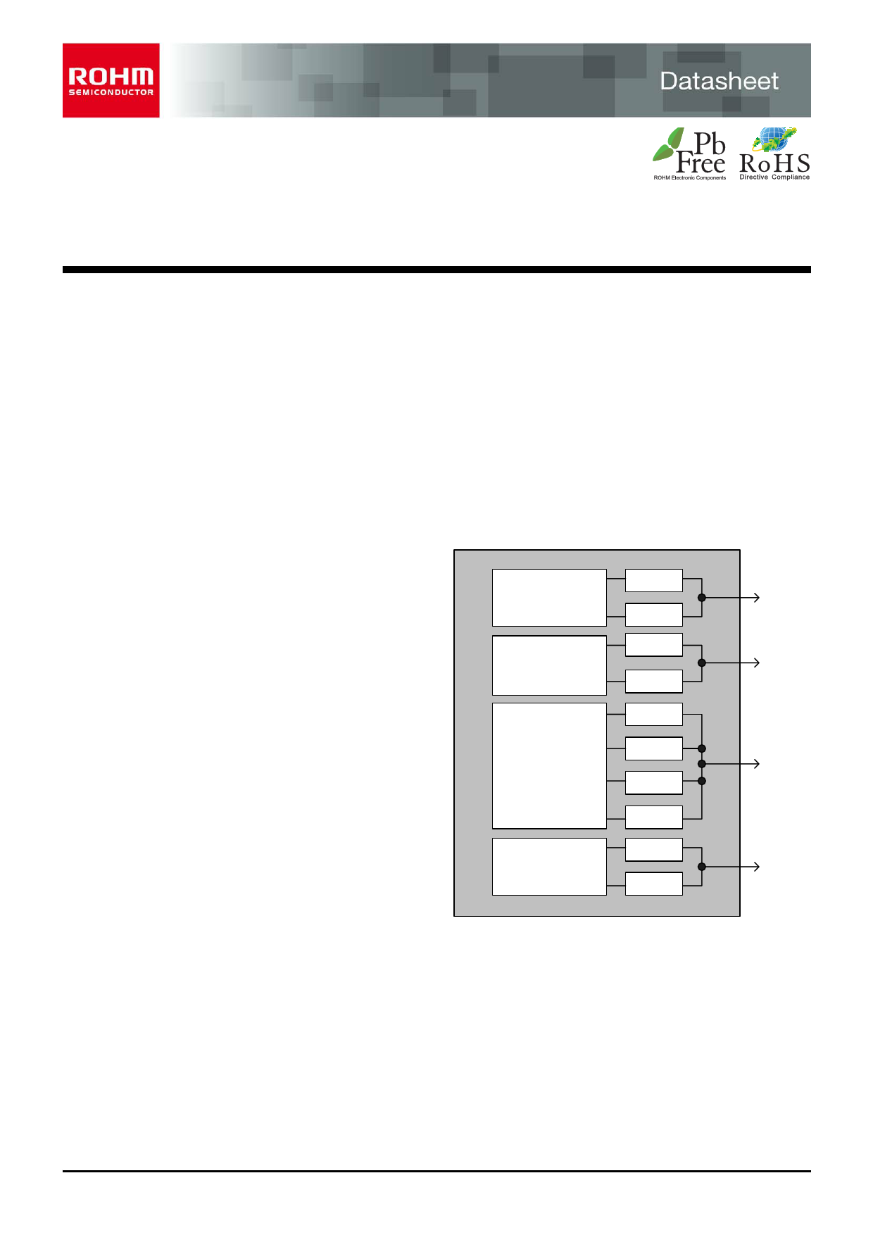
●Function block diagram
Step Down
DC/DC 1
Step Down
DC/DC 2
FET
FET
FET
FET
FET
Buck Boost
DC/DC 3
FET
FET
Step Down
DC/DC 4
FET
FET
FET
4.0V to 14.0V
0.6V±1.67% (typ.)
0.8V±1.25% (typ.)
0.8V±1.25% (typ.)
0.8V±1.25% (typ.)
3.0A(max)
2.0A(max)
1.5A(max)
3.0A(max)
1MHz(typ.)
1.1V
1.5V
5.0V
3.3V
Figure. 1 Function block diagram
○Product structure:Sillicon monolithic integrated circuit
www.rohm.com
© 2013 ROHM Co., Ltd. All rights reserved.
TSZ22111・14・001
○This product is not designed protection against radio active rays
1/35
TSZ02201-0B2B0A400010-1-2
17.APR.2013 Rev.001
1 page 
BD9866GUL
Datasheet
●Electrical Characteristics(Ta=25℃, VCC=PVCC=6V, RT=82kΩ, CTL1-4=3V, unless otherwise noted)
Parameter
Limits
Symbol
Units
Min Typ Max
Conditions
【Internal Regulator】
Regulator output voltage for internal
analog circuit
VREGA
3.3
3.5
3.7
V IVREGA=-1mA
Regulator output voltage for bias
voltage of Highside FET
VREGB VCC-3.7 VCC-3.5 VCC-3.3 V IVREGB=+1mA
Regulator output voltage for bias
voltage of Lowside FET
VREGD
3.3
3.5
3.7
V IVREGD=-1mA
【Under Voltage Lock Out】
Threshold voltage of VCC
undervoltage lock out
Hysteresis voltage of VCC
undervoltage lock out
Threshold voltage of VREG
undervoltage lock out
Hysteresis voltage of VREG
undervoltage lock out
【Short Circuit Protection】
VSTD1
3.2
3.4
3.6
V
VCC terminal voltage
monitor
VHYS1
-
0.1
0.2
V
VCC terminal voltage
monitor
VREGA,VREGD
VSTD2
2.8
3.0
3.2
V terminals voltage
monitor
VREGA,VREGD
VHYS2
-
0.1 0.2 V terminals voltage
monitor
SCP terminal output current
ISCP 2.5 5.0 7.5 µA VSCP=0.1V
SCP terminal detect voltage
VTSC 0.45 0.50 0.55 V
SCP terminal stand-by voltage
VSSC
-
10 100 mV
【Oscillator】
Oscillator frequency of DC/DC
converter
FOSC
0.9
1.0
1.1 MHz RT=82kΩ
Max duty Lx1,Lx2,Lx4
DMAX1,2,4
-
-
100
%
VSCP=0V (*4),
Lx1,Lx2,Lx4 High Duty
Max duty Lx31
DMAX31
-
- 100 % Lx31 High Duty
Max duty Lx32
DMAX32
74
80
86 % Lx32 Low Duty
RTSS terminal stand-by voltage
RTSSF
-
1 20 mV CTL1-4=0V
RTSS terminal input current
IRTSSI
-7
-5
-3 µA
RTSS terminal output current
IRTSSO
3
5
7 µA
【Error Amplifier】
INV1-4 terminal input bias current IINV1,2,3,4 -50 0 50 nA INV=2.0V
INV1 terminal threshold voltage
VINV1
0.590 0.600 0.610
V
INV2-4 terminal threshold voltage VINV2,3,4 0.790 0.800 0.810
V
【Soft Start】
CH1 Soft start time
TSS1 0.7 1.4 2.1 msec
CH2,3,4 Soft start time
TSS2,3,4 0.95 1.9 2.85 msec
(*4) SCP circuit starts to charge when operated 100% Duty, therefore it is possible to use 100% Duty only while SCP voltage doesn’t reach to 0.5V.
www.rohm.com
© 2013 ROHM Co., Ltd. All rights reserved.
TSZ22111・15・001
5/35
TSZ02201-0B2B0A400010-1-2
17.APR.2013 Rev.001
5 Page 
BD9866GUL
●Timing chart of SCP detection after startup
INV
EOUT
(internal node)
3.0V(typ.)
Datasheet
0.8V(setting voltage)
Output stops with SCP latch
SCP
Charge the capacitor
connected SCP terminal by
charge current of 5μA
0.5V(typ.)
SCP latch is detected when SCP > 0.5V
(Latch state is released at UVLO)
Latch detect time when capacitor connected
to SCP terminal is 0.01μF
PG =(C×V)/I
=(0.01μ×0.5)/5μ=1msec
Open drain terminal becomes Low by SCP latch
Figure. 8 Timing chart of SCP detection after startup
(abnormal output in operating)
www.rohm.com
© 2013 ROHM Co., Ltd. All rights reserved.
TSZ22111・15・001
11/35
TSZ02201-0B2B0A400010-1-2
17.APR.2013 Rev.001
11 Page | ||
| Páginas | Total 30 Páginas | |
| PDF Descargar | [ Datasheet BD9866GUL.PDF ] | |
Hoja de datos destacado
| Número de pieza | Descripción | Fabricantes |
| BD9866GUL | 4CH Internal Power MOSFET System Switching Regulator | ROHM Semiconductor |
| Número de pieza | Descripción | Fabricantes |
| SLA6805M | High Voltage 3 phase Motor Driver IC. |
Sanken |
| SDC1742 | 12- and 14-Bit Hybrid Synchro / Resolver-to-Digital Converters. |
Analog Devices |
|
DataSheet.es es una pagina web que funciona como un repositorio de manuales o hoja de datos de muchos de los productos más populares, |
| DataSheet.es | 2020 | Privacy Policy | Contacto | Buscar |