No Preview Available !

S25FL129P
128-Mbit 3.0 V Flash Memory
This product is not recommended for new and current designs. For new and current designs, S25FL128S supersedes S25FL129P.
This is the factory-recommended migration path. Please refer to the S25FL128S data sheet for specifications and ordering
information.
Distinctive Characteristics
Architectural Advantages
Single power supply operation
– Full voltage range: 2.7 to 3.6V read and write operations
Memory architecture
– Uniform 64 KB sectors
– Top or bottom parameter block (Two 64-KB sectors broken down
into sixteen 4-KB sub-sectors each)
– Uniform 256 KB sectors (no 4-KB sub-sectors)
– 256-byte page size
– Backward compatible with the S25FL128P (uniform 256 KB
sector) device
Program
– Page Program (up to 256 bytes) in 1.5 ms (typical)
– Program operations are on a page by page basis
– Accelerated programming mode via 9V W#/ACC pin
– Quad Page Programming
Erase
– Bulk erase function
– Sector erase (SE) command (D8h) for 64 KB and 256 KB sectors
– Sub-sector erase (P4E) command (20h) for 4 KB sectors
(for uniform 64-KB sector device only)
– Sub-sector erase (P8E) command (40h) for 8 KB sectors
(for uniform 64-KB sector device only)
Cycling endurance
– 100,000 cycles per sector typical
Data retention
– 20 years typical
Device ID
– JEDEC standard two-byte electronic signature
– RES command one-byte electronic signature for backward
compatibility
One time programmable (OTP) area for permanent, secure
identification; can be programmed and locked at the factory or by the
customer
CFI (Common Flash Interface) compliant: allows host system to
identify and accommodate multiple flash devices
Process technology
– Manufactured on 0.09 µm MirrorBit® process technology
Package option
– Industry Standard Pinouts
– 16-pin SO package (300 mils)
– 8-contact WSON package (6 x 8 mm)
– 24-ball BGA (6 x 8 mm) package, 5 x 5 pin configuration
– 24-ball BGA (6 x 8 mm) package, 6 x 4 pin configuration
Performance Characteristics
Speed
– Normal READ (Serial): 40 MHz clock rate
– FAST_READ (Serial): 104 MHz clock rate (maximum)
– DUAL I/O FAST_READ: 80 MHz clock rate or
20 MB/s effective data rate
– QUAD I/O FAST_READ: 80 MHz clock rate or
40 MB/s effective data rate
Power saving standby mode
– Standby Mode 80 µA (typical)
– Deep Power-Down Mode 3 µA (typical)
Memory Protection Features
Memory protection
– W#/ACC pin works in conjunction with Status Register Bits to
protect specified memory areas
– Status Register Block Protection bits (BP2, BP1, BP0) in status
Cypress Semiconductor Corporation • 198 Champion Court
Document Number: 002-00648 Rev. *I
• San Jose, CA 95134-1709 • 408-943-2600
Revised September 24, 2015

S25FL129P
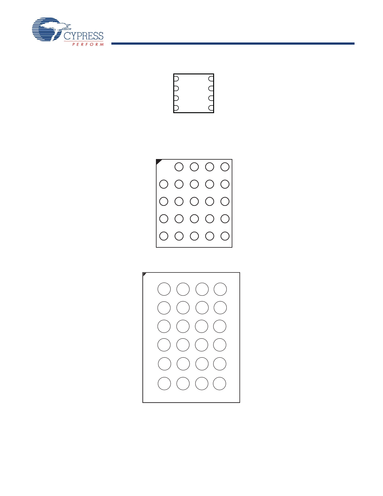
Figure 2.2 8-contact WSON Package (6 x 8 mm)
CS#
SO/IO1
W#/ACC/IO2
1
2
WSON
3
8
7
6
VCC
HOLD#/IO3
SCK
GND 4
5 SI/IO0
Note
There is an exposed central pad on the underside of the WSON package. This should not be connected to any voltage or signal line on the PCB. Connecting the central
pad to GND (VSS) is possible, provided PCB routing ensures 0mV difference between voltage at the WSON GND (VSS) lead and the central exposed pad.
Figure 2.3 6 x 8 mm 24-ball BGA Package, 5 x 5 Pin Configuration
12345
A
NC NC NC NC
B
NC
SCK GND VCC
NC
C
NC
CS#
NC W#/ACC/IO2 NC
D
NC SO/IO1 SI/IO0 HOLD#/IO3 NC
E
NC NC NC NC NC
Figure 2.4 6 x 8 mm 24-ball BGA Package, 6 x 4 Pin Configuration
A1 A2 A3 A4
NC NC NC NC
B1 B2 B3 B4
NC
SCK
GND
VCC
C1 C2
C3 C4
NC CS# NC W#/ACC/IO2
D1 D2 D3 D4
NC SO/IO1 SI/IO0 HOLD#/IO3
E1 E2 E3 E4
NC NC NC NC
F1 F2 F3 F4
NC NC NC NC
Document Number: 002-00648 Rev. *I
Page 6 of 66

S25FL129P
Note: It is suggested that the Block Protection and Parameter sectors not be set to the same area of the array; otherwise, the user
cannot utilize the Parameter sectors if they are protected. The following matrix shows the recommended settings.
TBPARM
0
0
1
1
TBPROT
0
1
0
1
Array Overview
Parameter Sectors - Bottom
BP Protection - Top (default)
Not recommended (Parameters and BP Protection are both Bottom)
Not recommended (parameters and BP Protection are both Top)
Parameter Sectors - Top of Array (high address)
BP Protection - Bottom of Array (low address)
Table 7.1 Configuration Register Table (Uniform 64 KB sector)
Bit Bit Name
Bit Function
Description
7 NA -
Not Used
6 NA -
Not Used
5 TBPROT Configures start of block protection
1 = Bottom Array (low address)
0 = Top Array (high address) (Default)
4 NA -
Do Not Use
3
BPNV
Configures BP2-0 bits in the Status Register
1 = Volatile
0 = Non-volatile (Default)
2 TBPARM Configures Parameter sector location
1 = Top Array (high address)
0 = Bottom Array (low address) (Default)
1
QUAD
Puts the device into Quad I/O mode
1 = Quad I/O
0 = Dual or Serial I/O (Default)
0 FREEZE Locks BP2-0 bits in the Status Register
1 = Enabled
0 = Disabled (Default)
Note
(Default) indicates the value of each Configuration Register bit set upon initial factory shipment.
Table 7.2 Configuration Register Table (Uniform 256 KB sector)
Bit Bit Name
Bit Function
Description
7 N/A -
Not Used
6 N/A -
Not Used
5
TBPROT
Configures start of block protection
1 = Bottom Array (low address)
0 = Top Array (high address) (Default)
4 N/A -
Do Not Use
3
BPNV
Configures BP2-0 bits in the Status Register
1 = Volatile
0 = Non-volatile (Default)
2 N/A -
Do not Use
1
QUAD
Puts the device into Quad I/O mode
1 = Quad I/O
0 = Dual or Serial I/O (Default)
0
FREEZE
Locks BP2-0 bits in the Status Register
1 = Enabled
0 = Disabled (Default)
Note
1. (Default) indicates the value of each Configuration Register bit set upon initial factory shipment.
Document Number: 002-00648 Rev. *I
Page 12 of 66


