|
|
|
PDF KAI-1010 Data sheet ( Hoja de datos )
| Número de pieza | KAI-1010 | |
| Descripción | Interline CCD Image Sensor | |
| Fabricantes | ON Semiconductor | |
| Logotipo | ||
Hay una vista previa y un enlace de descarga de KAI-1010 (archivo pdf) en la parte inferior de esta página. Total 27 Páginas | ||
|
No Preview Available !
KAI-1010
1008 (H) x 1018 (V) Interline
CCD Image Sensor
Description
The KAI−1010 Image Sensor is a high-resolution monochrome
charge coupled device (CCD) device whose non-interlaced
architecture makes it ideally suited for video, electronic still and
motion/still camera applications. The device is built using an
advanced true two-phase, double-polysilicon, NMOS CCD
technology. The p+npn− photodetector elements eliminate image lag
and reduce image smear while providing antiblooming protection and
electronic-exposure control. The total chip size is 10.15 (H) mm ×
10.00 (V) mm
Table 1. GENERAL SPECIFICATIONS
Parameter
Typical Value
Architecture
Interline CCD, Non-Interlaced
Total Number of Pixels
1024 (H) × 1024 (V)
Number of Effective Pixels
1008 (H) × 1018 (V)
Number of Active Pixels
1008 (H) × 1018 (V)
Number of Outputs
1 or 2
Pixel Size
9 mm (H) × 9 mm (V)
Active Image Size
9.1 mm (H) × 9.2 mm (V)
12.9 mm (Diagonal)
1″ Optical Format
Optical Fill-Factor
Saturation Signal
Output Sensitivity
Dark Noise
Dark Current
60%
> 50,000 e−
12 mV/e−
50 e− rms
< 0.5 nA/cm2
Quantum Efficiency
(Wavelength = 500 nm)
37%
Blooming Suppression
> 100 X
Maximum Data Rate
20 MHz/Channel (2 Channels)
Image Lag
Negligible
Package
CERDIP
Cover Glass
AR Coated (Both Sides)
NOTE: All Parameters are specified at T = 40°C unless otherwise noted.
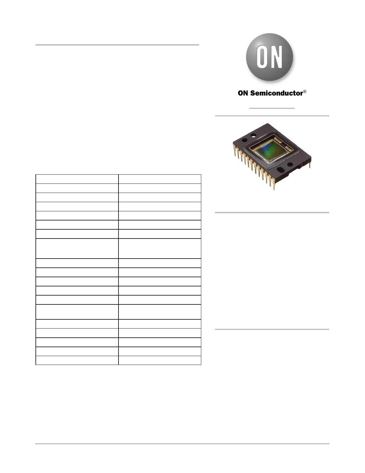
www.onsemi.com
Figure 1. KAI−1010 Interline
CCD Image Sensor
Features
• Front Illuminated Interline Architecture
• Progressive Scan (Non-Interlaced)
• Electronic Shutter
• On-Chip Dark Reference
• Low Dark Current
• High Sensitivity Output Structure
• Anti-Blooming Protection
• Negligible Lag
• Low Smear (0.1% with Microlens)
Application
• Machine Vision
ORDERING INFORMATION
See detailed ordering and shipping information on page 2 of
this data sheet.
© Semiconductor Components Industries, LLC, 2015
May, 2015 − Rev. 2
1
Publication Order Number:
KAI−1010/D
1 page 
KAI−1010
Output Structure
Charge packets contained in the horizontal register are
dumped pixel by pixel, onto the floating diffusion output
node whose potential varies linearly with the quantity of
charge in each packet. The amount of potential change is
determined by the expression DVFD = DQ / CFD. A three
stage source-follower amplifier is used to buffer this signal
voltage off chip with slightly less than unity gain. The
translation from the charge domain to the voltage domain is
quantified by the output sensitivity or charge to voltage
conversion in terms of mV/e−. After the signal has been
sampled off-chip, the reset clock (fR) removes the charge
from the floating diffusion and resets its potential to the
reset-drain voltage (VRD).
Electronic Shutter
The KAI−1010 provides a structure for the prevention of
blooming which may be used to realize a variable exposure
time as well as performing the anti-blooming function. The
anti-blooming function limits the charge capacity of the
photodiode by draining excess electrons vertically into the
substrate (hence the name Vertical Overflow Drain or
VOD). This function is controlled by applying a large
potential to the device substrate (device terminal SUB). If
a sufficiently large voltage pulse (VES ≈ 40 V) is applied to
the substrate, all photodiodes will be emptied of charge
through the substrate, beginning the integration period.
After returning the substrate voltage to the nominal value,
charge can accumulate in the diodes and the charge packet
is subsequently readout onto the VCCD at the next
occurrence of the high level on fV1. The integration time is
then the time between the falling edges of the substrate
shutter pulse and fV1. This scheme allows electronic
variation of the exposure time by a variation in the clock
timing while maintaining a standard video frame rate.
Application of the large shutter pulse must be avoided
during the horizontal register readout or an image artifact
will appear due to feedfthrough. The shutter pulse VES
must be “hidden” in the horizontal retrace interval.
The integration time is changed by skipping the shutter
pulse from one horizontal retrace interval to another.
The smear specification is not met under electronic shutter
operation. Under constant light intensity and spot size, if the
electronic exposure time is decreased, the smear signal will
remain the same while the image signal will decrease
linearly with exposure. Smear is quoted as a percentage of
the image signal and so the percent smear will increase by
the same factor that the integration time has decreased. This
effect is basic to interline devices.
Extremely bright light can potentially harm solid state
imagers such as Charge-Coupled Devices (CCDs). Refer to
Application Note Using Interline CCD Image Sensors in
High Intensity Visible Lighting Conditions.
www.onsemi.com
5
5 Page 
400
350
300
250
200
150
100
50
0
0
600
500
400
300
200
100
KAI−1010
(HSAT, VSAT)
0.1 0.2 0.3 0.4 0.5 0.6 0.7
Sensor Plane Irradiance − H − (arb)
Figure 9. Typical KAI−1010−ABA Photoresponse
0.8
VSUB = 8 V
VSUB = 9 V
VSUB = 10 V
VSUB = 11 V
VSUB = 12 V
VSUB = 13 V
VSUB = 14 V
VSUB = 15 V
0
0
0.1 0.2 0.3 0.4 0.5 0.6 0.7 0.8
Sensor Plane Irradiance − H − (arb)
Notes:
1. As VSUB is decreased, VSAT increases and anti-blooming protection decreases.
2. As VSUB is increased, VSAT decreases and anti-blooming protection increases.
Figure 10. Example of VSAT vs. VSUB
www.onsemi.com
11
0.9
11 Page | ||
| Páginas | Total 27 Páginas | |
| PDF Descargar | [ Datasheet KAI-1010.PDF ] | |
Hoja de datos destacado
| Número de pieza | Descripción | Fabricantes |
| KAI-1010 | Interline CCD Image Sensor | ON Semiconductor |
| KAI-10100 | Image Sensor | ON Semiconductor |
| Número de pieza | Descripción | Fabricantes |
| SLA6805M | High Voltage 3 phase Motor Driver IC. |
Sanken |
| SDC1742 | 12- and 14-Bit Hybrid Synchro / Resolver-to-Digital Converters. |
Analog Devices |
|
DataSheet.es es una pagina web que funciona como un repositorio de manuales o hoja de datos de muchos de los productos más populares, |
| DataSheet.es | 2020 | Privacy Policy | Contacto | Buscar |