|
|
|
PDF NCP4201 Data sheet ( Hoja de datos )
| Número de pieza | NCP4201 | |
| Descripción | Programmable Multi-Phase Synchronous Buck Converter | |
| Fabricantes | ON Semiconductor | |
| Logotipo | ||
Hay una vista previa y un enlace de descarga de NCP4201 (archivo pdf) en la parte inferior de esta página. Total 30 Páginas | ||
|
No Preview Available !
NCP4201
Programmable Multi-Phase
Synchronous Buck
Converter with PMBus
The NCP4201 is an integrated power control IC with a PMBus
interface. It combines a highly efficient, multi−phase, synchronous
buck switching regulator controller with a PMBus interface, which
enables digital programming of key system parameters to optimize
system performance and provide feedback to the system.
It uses an internal 8−bit DAC to read a Voltage Identification (VID)
code directly from the processor, which is used to set the output
voltage between 0.375 V and 1.6 V.
This device uses a multi−mode PWM architecture to drive the
logic−level outputs at a programmable switching frequency that can
be optimized for VR size and efficiency. The NCP4201 can be
programmed to provide 2−, 3−, or 4−phase operation, allowing for the
construction of up to four complementary buck−switching stages. The
NCP4201 supports PSI, which is a Power Save Mode.
The NCP4201 includes a PMBus interface which can be used to
program system set points such as voltage offset, load−line and phase
balance and output voltage. Key system performance data, such as
CPU current, CPU voltage, and power and fault conditions can also be
read back over the PMBus from the NCP4201.
The NCP4201 is specified over the extended commercial
temperature range of 0°C to +85°C and is available in a 40 Lead QFN
package.
Features
• Selectable 2−, 3−, or 4−Phase Operation at Up to 1.5 MHz per Phase
• PMBus Interface − Enables Digital Programmability of Set Points
and Read−back of Monitored Values
• Logic−Level PWM Outputs for Interface to External High Power
Drivers
• Fast−Enhanced PWM for Excellent Load Transient Performance
• Active Current Balancing Between All Output Phases
• Built−In Power−Good/Crowbar Blanking Supports On−The−Fly
(OTF) VID Code Changes
• Digitally Programmable 0.375 V to 1.6 V Output Supports Both
VR11 and VR11.1 Specifications
• Programmable Short−Circuit Protection with Programmable
Latchoff Delay
• Supports PSI – Power Saving Mode During Light Loads
Applications
• Desktop PC Power Supplies for VRM Modules
© Semiconductor Components Industries, LLC, 2009
September, 2009 − Rev. 0
1
http://onsemi.com
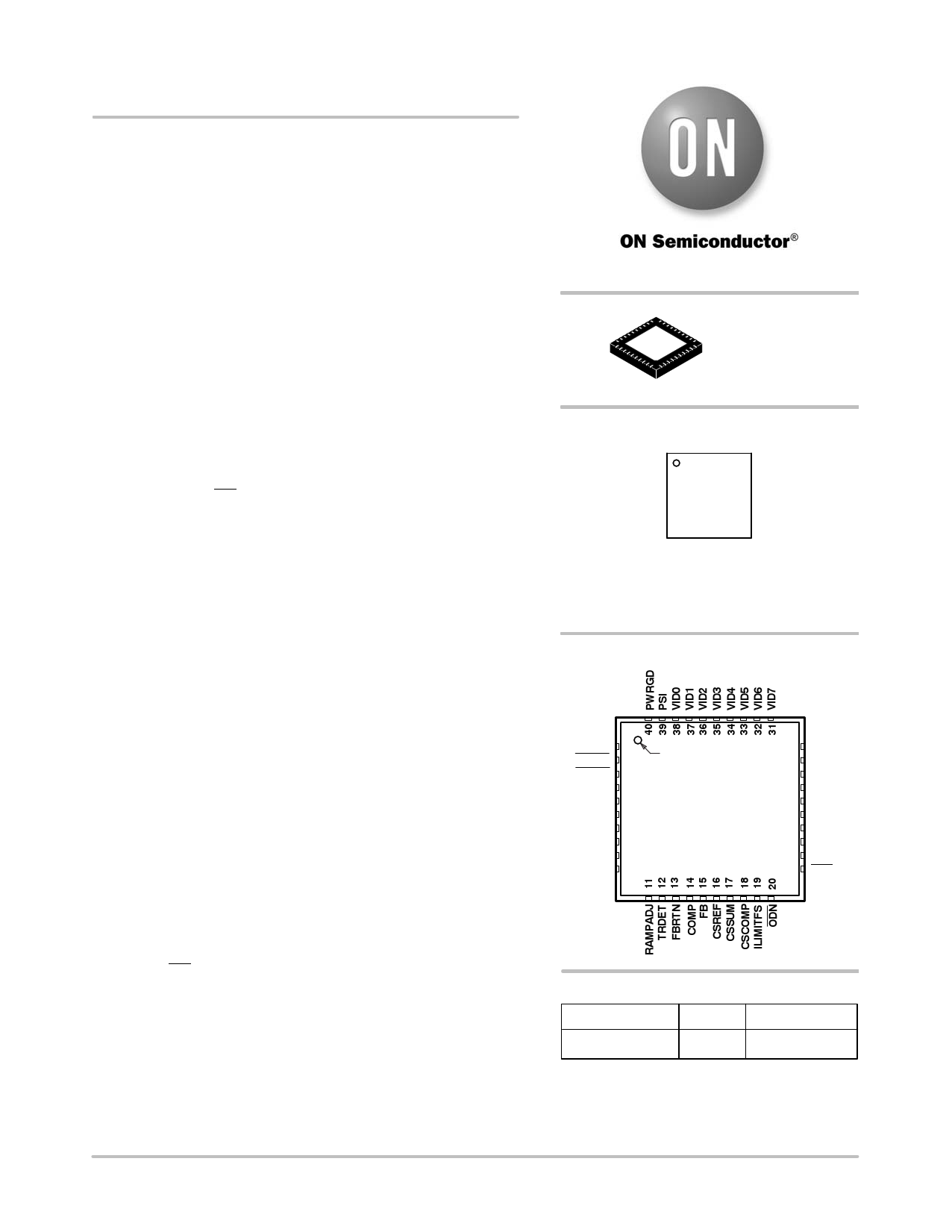
1 40
QFN40 6x6
CASE 488AR
MARKING DIAGRAM
NCP4201
AWLYYWWG
A = Assembly Location
WL = Wafer Lot
YYWW = Date Code
G = Pb−Free Package
PIN ASSIGNMENT
VCC3
ALERT
FAULT
SDA
SCL
EN
GND
IMON
IREF
RT
1
2
3
4
5
6
7
8
9
10
PIN 1
INDICATOR
NCP4201
TOP VIEW
30 VCC
29 PWM1
28 PWM2
27 PWM3
26 PWM4
25 SW1
24 SW2
23 SW3
22 SW4
21 OD1
ORDERING INFORMATION
Device*
Package
Shipping†
NCP4201MNR2G QFN40 2500/Tape & Reel
*The “G’ suffix indicates Pb−Free package.
†For information on tape and reel specifications,
including part orientation and tape sizes, please
refer to our Tape and Reel Packaging Specifications
Brochure, BRD8011/D.
Publication Order Number:
NCP4201/S
1 page 
NCP4201
PIN FUNCTION DESCRIPTIONS
Pin No
1
Mnemonic
VCC3
Description
3.3 V Power Supply Output. A capacitor from this pin to ground provided decoupling for the interval
3.3 V LDO.
2
ALERT
ALERT Output. Open drain output that asserts low when the VR exceeds a programmable limit.
3
FAULT
FAULT Output. Open drain output that asserts low when a fault has occurred. The fault can be due to
VR or current limit, crowbar, or undervoltage. The trip points are loaded into registers.
4
SDA
Digital Input/Output. PMBus serial data bidirectional pin. Requires PMBus pullup.
5 SCL Digital Input. PMBus serial bus clock open drain input. Requires PMBus pullup.
6 EN Power Supply Enable Input. Pulling this pin to GND disables the PWM outputs and pulls the
PWRGD output low.
7
GND
Ground. All internal biasing and the logic output signals of the device are referenced to this ground.
8
IMON
Analog Filter Output. A capacitor from this pin to ground sets the default current monitor filter
frequency. The frequency can be modified using the serial interface.
9
IREF
Current Reference Input. An external resistor from this pin to ground sets the reference current for
IFB, IILIMITFS and ITH(X).
10 RT Frequency Setting Resistor Input. An external resistor connected between this pin and GND sets the
oscillator frequency of the device.
11
RAMPADJ
PWM Ramp Current Input. An external resistor from the converter input voltage to this pin sets the
internal PWM ramp.
12
TRDET
Transient Detect.
13
FBRTN
Feedback Return. VID DAC and error amplifier reference for remote sensing of the output voltage.
14
COMP
Error Amplifier Output and Compensation Point.
15 FB Feedback Input. Error amplifier input for remote sensing of the output voltage. An external resistor
between this pin and the output voltage sets the no load offset point.
16
CSREF
Current Sense Reference Voltage Input. The voltage on this pin is used as the reference for the
current sense amplifier and the power−good and crowbar functions. This pin should be connected to
the common point of the output inductors.
17
CSSUM
Current Sense Summing Node. External resistors from each switch node to this pin sum the average
inductor currents together to measure the total output current.
18
CSCOMP
Current Sense Compensation Point. A resistor and capacitor from this pin to CSSUM determines the
gain of the current sense amplifier and the positioning loop response time.
19
ILIMITFS
Current Sense and Limit Scaling Pin. An external resistor from this pin to CSCOMP sets the internal
current sensing signal for current limit and IMON. This value can be overwritten using the PMBus
interface.
20
ODN
Output Disable Logic Output for phases 2−4. This pin is actively pulled low when the EN input is low
or when VCC is below its UVLO threshold to signal to the Driver IC that the driver high−side and
low−side outputs should go low.
21
OD1
Output Disable Logic Output for phase one. This pin is actively pulled low when the EN input is low
or when VCC is below its UVLO threshold to signal to the Driver IC that the driver high−side and
low−side outputs should go low.
22 to 25
SW4 to SW1
Current Balance Inputs. Inputs for measuring the current level in each phase. The SW pins of
unused phases should be left open.
26 to 29
PWM4 to PWM1
Logic−Level PWM Outputs. Each output is connected to the input of an external MOSFET driver
such as the ADP3121. Connecting the PWM4, and PWM3 outputs to VCC causes that phase to turn
off, allowing the NCP4201 to operate as a 2−phase controller.
30
31 to 38
VCC
VID7 to VID0
Supply Voltage for the Device.
Voltage Identification DAC Inputs. These eight pins are pulled down to GND, providing a logic zero if
left open. When in normal operation mode, the DAC output programs the FB regulation voltage from
0.375 V to 1.6 V.
39 PSI Power Save Interface. System signal to select single phase option.
40
PWRGD
Power−Good Output. Open−drain output that signals when the output voltage is outside of the proper
operating range.
http://onsemi.com
5
5 Page 
NCP4201
Description
The NCP4201 is a 4 Phase DC−DC regulator with a
PMBus Interface. A typical application circuit is shown in
Figure 2.
Startup Sequence
The NCP4201 follows the startup sequence shown in
Figure 7. After both the EN and UVLO conditions are met,
a programmable internal timer goes through one delay cycle
TD1. This delay cycle is programmed using Delay
Command, default delay = 2 ms, see Table 2 for
programmable values. The first six clock cycles of TD2 are
blanked from the PWM outputs and used for phase detection
as explained in the following section. Then the
programmable internal soft−start ramp is enabled (TD2) and
the output comes up to the boot voltage of 1.05 V. The boot
hold time is also set by Delay Command. This second delay
cycle is called TD3. During TD3 the processor VID pins
settle to the required VID code. When TD3 is over, the
NCP4201 reads the VID inputs and soft−starts either up or
down to the final VID voltage (TD4). After TD4 has been
completed and the PWRGD masking time (equal to VID
OTF masking) is finished, a third cycle of the internal timer
sets the PWRGD blanking (TD5).
The internal delay and soft−start times are programmable
using the serial interface, the Delay Command and the
Soft−Start Commands.
5.0 V
SUPPLY
UVLO
THRESHOLD
VTT I/O
(NCP4201 EN)
VCC_CORE
VR READY
(NCP4201 PWRGD)
CPU
VID INPUTS
0.85 V
TD1
TD3
VBOOT
(1.05 V)
TD2
V VID
TD4
VID INVALID
50 ms
TD5
VID VALID
Figure 7. Startup Sequence
Internal Delay Timer
An internal timer sets the delay times for the start up
sequence, TD1, TD3 and TD5. The default time is 2 msec,
which can be changed using the PMBus interface. This timer
is used for multiple delay timings (TD1, TD3 and TD5)
during the startup sequence. Also, it is used for timing the
current limit latchoff as explained in the Current Limit
section. The current limit timer is set to 4 times the delay
timer.
The delay timer is programmed using Bits <2:0> of the
Ton Delay command (0xD4). The delay can be programmed
between 0.5 msec and 4 msec. Table 1 provides the
programmable delay times.
Table 1. Delay Codes
Code
000
001
010
011
100
101
110
111
Delay (msec)
0.5
1
1.5
2 = default
2.5
3
3.5
4
Soft−Start
The Soft−Start slope for the output voltage is set by an
internal timer. The default value is 0.5 V/msec, which can be
programmed through the PMBus interface. After TD1 and
the phase detection cycle have been completed, the SS time
(TD2 in Figure 2) starts. The SS uses the internal VID DAC
to increase the output voltage in 6.25 mV steps up to the
1.05 V boot voltage.
Once the SS circuit has reached the boot voltage, the boot
voltage delay time (TD3) is started. The end of the boot
voltage delay time signals the beginning of the second
soft−start time (TD4). The SS voltage changes from the boot
voltage to the programmed VID DAC voltage (either higher
or lower) using 6.25 mV steps.
The soft−start slew rate is programmed using Bits <2:0>
of the Ton_Rise (0xD5) command code. Table 2 provides
the soft−start values.
Table 2. Slew Rate Codes
Code
000
001
010
011
100
101
110
111
Slew Rate (V/msec)
0.1
0.3
0.5 = default
0.7
0.9
1.1
1.3
1.5
http://onsemi.com
11
11 Page | ||
| Páginas | Total 30 Páginas | |
| PDF Descargar | [ Datasheet NCP4201.PDF ] | |
Hoja de datos destacado
| Número de pieza | Descripción | Fabricantes |
| NCP4200 | Programmable Multi-Phase Synchronous Buck Converter | ON Semiconductor |
| NCP4201 | Programmable Multi-Phase Synchronous Buck Converter | ON Semiconductor |
| NCP4206 | VR11.1 Digital Programmable Multi-Phase Synchronous Buck Converter | ON Semiconductor |
| NCP4208 | VR11.1 Digital Programmable 8-Phase Synchronous Buck Converter | ON Semiconductor |
| Número de pieza | Descripción | Fabricantes |
| SLA6805M | High Voltage 3 phase Motor Driver IC. |
Sanken |
| SDC1742 | 12- and 14-Bit Hybrid Synchro / Resolver-to-Digital Converters. |
Analog Devices |
|
DataSheet.es es una pagina web que funciona como un repositorio de manuales o hoja de datos de muchos de los productos más populares, |
| DataSheet.es | 2020 | Privacy Policy | Contacto | Buscar |