|
|
|
PDF FPC1011F3 Data sheet ( Hoja de datos )
| Número de pieza | FPC1011F3 | |
| Descripción | Area Sensor Package | |
| Fabricantes | FINGERPRINTS | |
| Logotipo | ||
Hay una vista previa y un enlace de descarga de FPC1011F3 (archivo pdf) en la parte inferior de esta página. Total 30 Páginas | ||
|
No Preview Available !
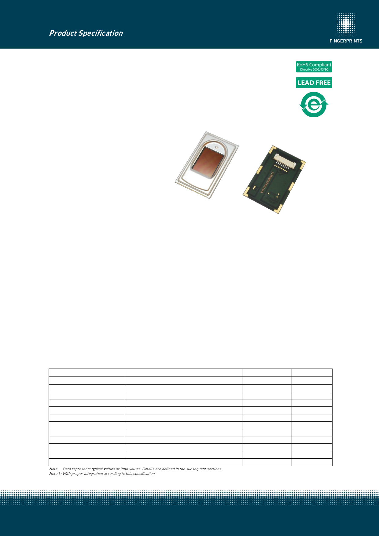
FPC1011F3 Area Sensor Package
Product Specification
Features
Fingerprint area sensor
Hard and scratch resistant protective surface coating
Superior image quality
3D image with 256 true gray scale values
Ergonomic frame for optimized finger guidance
High speed SPI interface
New ultra-thin flex film connector
2.5 to 3.3 volt operation
Extended ESD range 30kV
>10 million finger placements
Application examples
Computer peripheral
Physical access control
Time and attendance
Wireless devices
Security application
Medical equipment & storage
General description
FPC1011F3 is a new compact CMOS fingerprint sensor with several significant advantages. FPC1011F3
delivers superior image quality, with 256 gray scale values in every single pixel. The reflective measurement
method sends an electrical signal via the frame directly into the finger. This technique enables the use of an
unbeatably hard and thick protective sensor surface coating. The sensor with its 3D pixel sensing technology
can read virtually any finger; dry or wet.
Thanks to the hard and durable surface coating, FPC1011F3 is protected against ESD above 30 kV, as well
as scratches, impact and everyday wear-and-tear. The FPC1011F3 includes a designed micro-ergonomic
guidance frame, supporting easy integration, simplifying proper fingerprint guidance and hence improving
algorithm performance.
The FPC1011F3 sensor also includes an ultra-thin flex film connector, supporting a high speed 4 pin serial
SPI interface.
Quick reference data
PARAMETER
DESCRIPTION
Sensor dimension
Sensor body (W x L x T), nominal
Interface
Flex connector, 4 pin SPI
Supply voltage
DC voltage, typical
Supply current
Typical at 3.3V, 4MHz and RT (room temp)
Supply current sleep mode
Power down, typical
Clock frequency
Serial SPI
Read out speed
Serial SPI
Active sensing area
Pixel matrix
Size sensing array
Pixel matrix (363 dpi)
Pixel resolution
256 gray scale values
ESD protection 1
IEC61000-4-2, level X, air discharge
Wear-and-tear
Finger placements
Note: Data represents typical values or limit values. Details are defined in the subsequent sections.
Note 1: With proper integration according to this specification.
VALUE
20.4 x 33.4 x 2.3
8
2.5 - 3.3
7
10
32
4
10.64 x 14.00
152 x 200
8
± 30
> 10 million
UNIT
mm
pin
V
mA
µA
MHz
Mpixel/s
mm
Pixel
Bit
kV
times
This specification is subject to changes without prior notice
www.fingerprints.com
1
710-FPC1011F3_C_Product-specification.docx
1 page 
FPC1011F3 Area Sensor Package
Product Specification
2 Electrical characteristics
Measured at room temperature (RT)
SYMBOL PARAMETER
CONDITION
MIN
TYP
MAX
UNIT
FPC1011F3
VDD Voltage supply (total)
IDD Current supply, total 1,3
FPC1011F3 - digital inputs
VDD = 2.5V@4MHz
VDD = 2.5V@32MHz
VDD = 3.3V@4MHz
VDD = 3.3V@32MHz
2.35 2
-
-
-
-
2.5 - 3.3
7
9
7
12
3.45
-
-
14
-
V
mA
mA
mA
mA
VIL Logic ’0’ voltage
VIH Logic ’1’ voltage
IIL Logic ’0’ current (VI = GND)
IIH Logic ’1’ current (VI = VDD)
CIND Input capacitance
FPC1011F3 - digital outputs
N/A N/A 0.2VDD V
0.8VDD
N/A
N/A
V
- - ±10 uA
- - ±10 uA
- 6 - pF
VOL Logic ’0’ output voltage
- 0.2 0.4 V
VOH Logic ’1’ output voltage
0.85VDD
0.90VDD
-
V
Note 1: Details on clock frequency are available in the General Timing section.
Note 2: Represents MIN voltage for the sensor die. Current consumption and hence the incoming voltage drop will increase with clock frequency, se Block diagram.
Note 3: Current values given above correspond to the average value measured over a 100ms time frame, during image readout.
The graph shows the typical supply
disturbance level (sinus rms), which
will give less than one gray level rms
disturbance in the fingerprint image
readout. If the supply voltage is
noisy, additional filtering may be
required.
Typical differential power supply disturbance
This specification is subject to change without prior notice
www.fingerprints.com
5
710-FPC1011F3_C_Product-specification.docx
5 Page 
FPC1011F3 Area Sensor Package
Product Specification
Read sensor instruction
INSTRUCTION
Mode
rd_sensor
serial
( 11H )
Input parameters 1 dummy byte
Data delay1
Returned bytes
(363±2)tCLK
0
Note1: Data delay is the delay time from when the
instruction is given, until data is available in
the FIFO.
This instruction is used to read the entire sensor or a
part of it. Timing for reading in serial mode is defined
in the section Timing properties.
The read sensor instruction is only used to start the
sense-sequence, and the instruction itself does not
return any data. The first data from the sensor array
will enter the FIFO after approximately 363 clock-
cycles. After that, a new byte will enter the FIFO every
8th clock-cycle until the area defined by the XSENSE,
YSENSE, XSHIFT and YSHIFT registers has been read.
Read SPI data instruction
INSTRUCTION
rd_spidata
Mode
serial
Input parameters 1 dummy byte
Data delay
0
Returned bytes
n
( 20H )
After the read SPI data instruction is sent,
<rd_spidata>, pixel data will be returned as shown in
Figure 11. Data will continue to be returned as long
as SPI_CS_N and SPI_DI are kept low.
SPI_DI should be kept low after the <rd_spidata>,
instruction is entered to avoid the subsequent byte
to be interpreted as a new instruction.
The reading of data can be stopped at any time
without data-loss by setting SPI_CS_N high, as long
as SPI_CS_N is set high between the last bit of the
current byte being read and the first bit in the next
byte.
When the FIFO is filled to a level equal to or greater
than the value set by the FIFO_TH register, the
SPI_STAT register will indicate that data is ready for
fetching.
If the FIFO is filled up with data, overflow is avoided
by stalling sensing until data is read from the FIFO.
During this stall-period all analog modules are active,
and the ASIC will draw current as during a regular
sense operation.
If SPI_CS_N is released at any other time (e.g.
during a byte transfer) one or more bytes will be
lost. To continue readout after a stop caused by
setting SPI_CS_N high, the <rd_spidata> instruction
has to be applied again.
This specification is subject to change without prior notice
www.fingerprints.com
11
710-FPC1011F3_C_Product-specification.docx
11 Page | ||
| Páginas | Total 30 Páginas | |
| PDF Descargar | [ Datasheet FPC1011F3.PDF ] | |
Hoja de datos destacado
| Número de pieza | Descripción | Fabricantes |
| FPC1011F | Area Sensor Package | FINGERPRINTS |
| FPC1011F3 | Area Sensor Package | FINGERPRINTS |
| Número de pieza | Descripción | Fabricantes |
| SLA6805M | High Voltage 3 phase Motor Driver IC. |
Sanken |
| SDC1742 | 12- and 14-Bit Hybrid Synchro / Resolver-to-Digital Converters. |
Analog Devices |
|
DataSheet.es es una pagina web que funciona como un repositorio de manuales o hoja de datos de muchos de los productos más populares, |
| DataSheet.es | 2020 | Privacy Policy | Contacto | Buscar |