|
|
|
PDF LC87F1JJ2A Data sheet ( Hoja de datos )
| Número de pieza | LC87F1JJ2A | |
| Descripción | 8-bit 1-chip Microcontroller | |
| Fabricantes | ON Semiconductor | |
| Logotipo | ||
Hay una vista previa y un enlace de descarga de LC87F1JJ2A (archivo pdf) en la parte inferior de esta página. Total 27 Páginas | ||
|
No Preview Available !
Ordering number : ENA1453A
LC87F1JJ2A
CMOS IC
FROM 192K byte, RAM 16384 byte on-chip
8-bit 1-chip Microcontroller
with USB-host controller
http://onsemi.com
Overview
The LC87F1JJ2A is an 8-bit microcomputer that, integrates on a single chip a number of hardware features such as
192K-byte flash ROM, 16384-byte RAM, an on-chip debugger, a 16-bit timer/counter, a 16-bit timer, four 8-bit
timers, a base timer serving as a realtime clock, 3 channels of synchronous SIO interface with automatic data transfer
capabilities, an asynchronous/synchronous SIO interface, a UART interface, a full-speed USB interface (host control
function), a 12-channel AD converter, 2 channels of 12-bit PWM, a system clock frequency divider, an infrared
remote control receiver circuit, and an interrupt feature.
Features
Flash ROM
• 196608 × 8 bits
• Capable of on-board programming
with a wide range of supply voltages: 3.0 to 5.5V
• Block-erasable in 128 byte units
• Writes data in 2-byte units
RAM
• 16384 × 9 bits
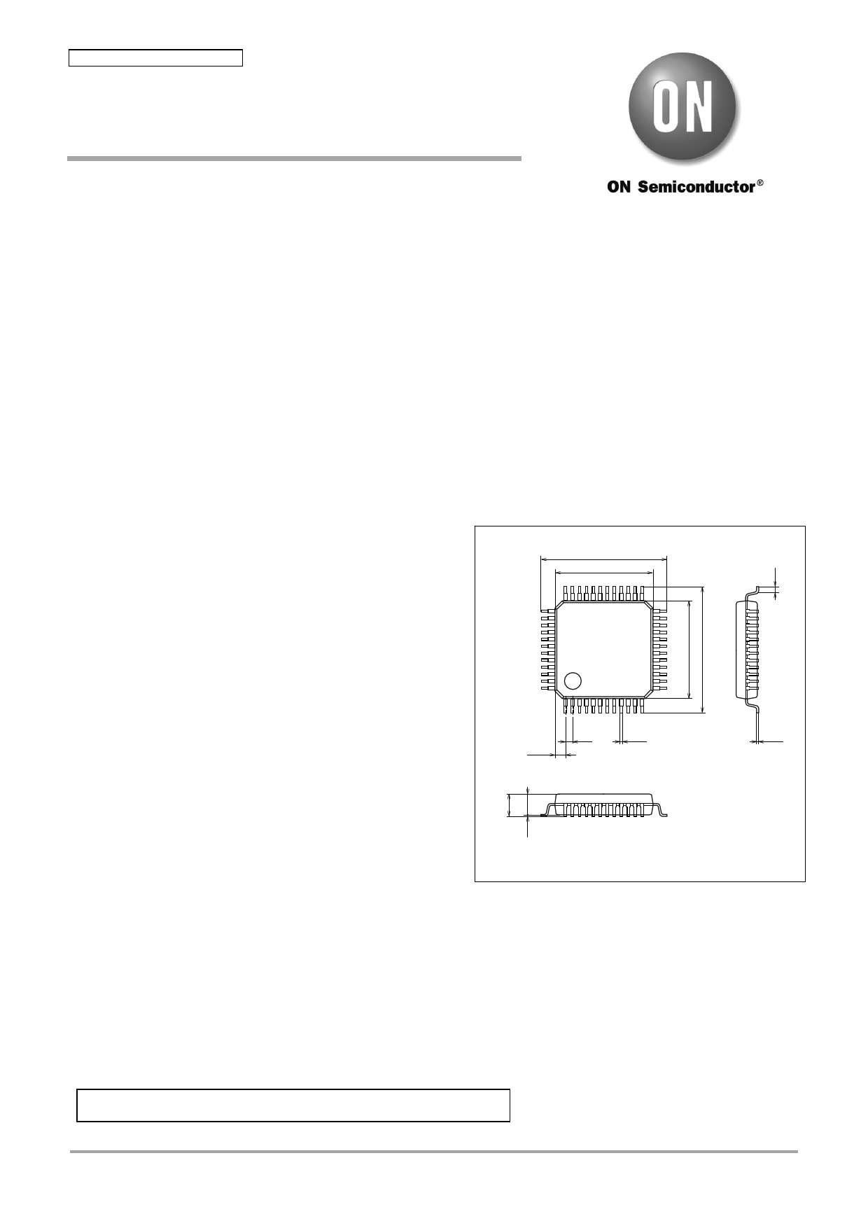
Package Form
• SQFP48(7×7): Lead-/Halogen-free type
Package Dimensions
unit : mm (typ) 3163B
9.0
7.0
36 25
37 24
48
1
(0.75)
0.5
13
12
0.18
0.15
SANYO : SQFP48(7X7)
* This product is licensed from Silicon Storage Technology, Inc. (USA).
Semiconductor Components Industries, LLC, 2013
May, 2013
Ver.1.02
D2612HK/52009HKIM 20090407-S00002 No.A1453-1/27
1 page 
LC87F1JJ2A
Standby Function
• HALT mode: Halts instruction execution while allowing the peripheral circuits to continue operation.
1) Oscillation is not halted automatically.
2) There are three ways of releasing the HALT mode.
(1) Setting the reset pin to the lower level.
(2) System resetting by watchdog timer
(3) Generating an interrupt
• HOLD mode: Suspends instruction execution and the operation of the peripheral circuits.
1) The PLL base clock generator, CF, RC and crystal oscillators automatically stop operation.
2) There are five ways of releasing the HOLD mode.
(1) Setting the reset pin to the lower level
(2) System resetting by watchdog timer
(3) Having an interrupt source established at one of the INT0, INT1, INT2, INT4, and INT5 pins
* The INT0 and INT1 pins must be configured only for level detection.
(4) Having an interrupt source established at port 0
(5) Having an bus active interrupt source established in the USB host control circuit
• X'tal HOLD mode: Suspends instruction execution and the operation of the peripheral circuits except the base timer.
1) The PLL base clock generator, CF and RC oscillator automatically stop operation.
2) The state of crystal oscillation established when the X'tal HOLD mode is entered is retained.
3) There are seven ways of releasing the X'tal HOLD mode.
(1) Setting the reset pin to the low level
(2) System resetting by watchdog timer
(3) Having an interrupt source established at one of the INT0, INT1, INT2, INT4, and INT5 pins
* The INT0 and INT1 pins must be configured only for level detection.
(4) Having an interrupt source established at port 0
(5) Having an interrupt source established in the base timer circuit
(6) Having an bus active interrupt source established in the USB host control circuit
(7) Having an interrupt source established in the infrared remote controller receiver circuit
Development Tools
• On-chip debugger: TCB87- type B + LC87F1JJ2A
Flash ROM Programming Boards
Package
Programming board
SQFP48(7×7)
W87F55256SQ
Flash ROM Programmer
Maker
Model
Supported Version
Device
Flash Support Group, Inc.
(FSG)
Single
AF9708/
AF9709/AF9709B/AF9709C
(including Ando Electric Co., Ltd. models)
Rev. 03.12 or later
LC87F1JJ2A
Flash Support Group, Inc.
(FSG)
+
Our company(Note 1)
Onboard
single/ganged
AF9101/AF9103(main unit)
(FSG)
SIB87(interface driver)
(Our company model)
(Note 2)
LC87F1JJ2A
Our company
Single/ganged
Onboard
single/ganged
SKK/SKK Type B
(SANYO FWS)
SKK-DBG Type B
(SANYO FWS)
Application version:
1.04 or later
Chip data version:
2.17 or later
LC87F1JJ2
Note 1: PC-less standalone onboard programming is possible using the FSG onboard programmer (AF9101/AF9103)
and the serial interface driver (SIB87) provided by Our company in pair.
Note 2: Dedicated programming device and program are required depending on the programming conditions. Contact
Our company or FSG if you have any questions or difficulties regarding this matter.
No.A1453-5/27
5 Page 
LC87F1JJ2A
USB Reference Power Option
When a voltage 4.5 to 5.5V is supplied to VDD1 and the internal USB reference voltage circuit is activated, the
reference voltage for USB port output is generated. The active/inactive state of the reference voltage circuit can be
switched by optional settings. The procedure for marking the optional settings is described below.
(1) (2) (3) (4)
Option settings
USB regulator
Use Use Use Nonuse
USB regulator in HOLD mode
Use
Nonuse
Nonuse
Nonuse
USB regulator in HALT mode
Use Nonuse Use Nonuse
Reference voltage circuit state
Normal mode
Active
Active
Active
Inactive
HOLD mode
Active
Inactive
Inactive
Inactive
HALT mode
Active
Inactive
Active
Inactive
• When the USB reference voltage circuit is made inactive, the level of the reference voltage for USB port output is
equal to VDD1.
• Selection (2) or (3) can be used to set the reference voltage circuit inactive in HOLD or HALT mode.
• When the reference voltage circuit is activated, the current drain increases by approximately 100μA compared with
when the reference voltage circuit is inactive.
Circuit example 1: When VDD1=VDD2=3.3V
• Inactivating the reference voltage circuit (selection (4)).
• Connecting VDD3 to VDD1 and VDD2.
Power supply
3.3V
2.2μF *1
LSI
VDD1
VDD2
VDD3
UHD+
UHD-
UFILT
VSS1 VSS2 VSS3
33Ω To USB connector
5pF 15kΩ
0Ω
2.2μF
*1: Needs adjustment on target board.
Circuit example 2: When VDD1=VDD2=5.0V
• Activating the reference voltage circuit (selection (1)).
• Isolating VDD3 from VDD1 and VDD2, and connecting capacitor between VDD3 and VSS.
Power supply
5V
2.2μF
LSI
VDD1
VDD2
UHD+
UHD-
VDD3
UFILT
0.1μF
VSS1 VSS2 VSS3
33Ω
5pF
To USB connector
15kΩ
0Ω
2.2μF
No.A1453-11/27
11 Page | ||
| Páginas | Total 27 Páginas | |
| PDF Descargar | [ Datasheet LC87F1JJ2A.PDF ] | |
Hoja de datos destacado
| Número de pieza | Descripción | Fabricantes |
| LC87F1JJ2A | 8-bit 1-chip Microcontroller | Sanyo Semicon Device |
| LC87F1JJ2A | 8-bit 1-chip Microcontroller | ON Semiconductor |
| LC87F1JJ2B | 8-bit 1-chip Microcontroller | Sanyo Semicon Device |
| Número de pieza | Descripción | Fabricantes |
| SLA6805M | High Voltage 3 phase Motor Driver IC. |
Sanken |
| SDC1742 | 12- and 14-Bit Hybrid Synchro / Resolver-to-Digital Converters. |
Analog Devices |
|
DataSheet.es es una pagina web que funciona como un repositorio de manuales o hoja de datos de muchos de los productos más populares, |
| DataSheet.es | 2020 | Privacy Policy | Contacto | Buscar |