|
|
|
PDF KAF-4320 Data sheet ( Hoja de datos )
| Número de pieza | KAF-4320 | |
| Descripción | CCD IMAGE SENSOR | |
| Fabricantes | ON Semiconductor | |
| Logotipo | ||
Hay una vista previa y un enlace de descarga de KAF-4320 (archivo pdf) en la parte inferior de esta página. Total 25 Páginas | ||
|
No Preview Available !
KAF-4320
2084 (H) x 2085 (V) Full
Frame CCD Image Sensor
Description
The KAF−4320 Image Sensor is a high performance monochrome
area CCD (charge-coupled device) image sensor designed for a wide
range of image sensing applications.
The sensor incorporates true two-phase CCD technology,
simplifying the support circuits required to drive the sensor as well as
reducing dark current without compromising charge capacity.
The sensor also utilizes the TRUESENSE Transparent Gate Electrode
to improve sensitivity compared to the use of a standard front side
illuminated polysilicon electrode.
The full imaging array is read out of four outputs, each of which is
driven by a low impedance two stage source follower that provides
a high conversion gain. This combination enables low noise at a net
readout rate of 12 MHz (3 MHz per output).
Table 1. GENERAL SPECIFICATIONS
Parameter
Typical Value
Architecture
Full Frame CCD
Total Number of Pixels
2092 (H) × 2093 (V)
Number of Active Pixels
2084 (H) × 2085 (V) = approx. 4.3 Mp
Pixel Size
24 mm (H) × 24 mm (V)
Active Image Size
50.02 mm (H) × 50.02 mm (V)
70.7 mm (Diagonal)
645 Optical Format
Die Size
Output Sensitivity
52.3 mm (H) × 52.7 mm (V)
10 mV/e−
Saturation Signal
500,000 electrons
Readout Noise
20 electrons (3 MHz)
Outputs
Dark Current
4
< 15 pA/cm2
Dark Current Doubling
Temperature
6.4°C
Dynamic Range
20,000 : 1
Blooming Suppression
None
Maximum Date Rate
3 MHz
Package
PGA Package
Cover Glass
Clear
NOTE: Parameters above are specified at T = 25°C unless otherwise noted.
www.onsemi.com
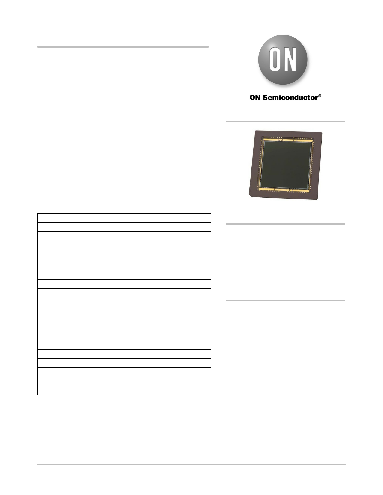
Figure 1. KAF−4320 Full Frame CCD
Image Sensor
Features
• True Two Phase Full Frame Architecture
• TRUESENSE Transparent Gate Electrode
for High Sensitivity
Applications
• Medical Imaging
• Scientific Imaging
ORDERING INFORMATION
See detailed ordering and shipping information on page 2 of
this data sheet.
© Semiconductor Components Industries, LLC, 2015
April, 2015 − Rev. 2
1
Publication Order Number:
KAF−4320/D
1 page 
Physical Description
Pin Description and Device Orientation
KAF−4320
61 60 59 58 57 56 55 54 53
VRD
VLG
VSS
GND
62
63
64
65
VOUT4 66
VDD 67
fV2 68
fV1 69
GND 70
fV1 71
fV2 72
GUARD 73
fV2 74
fV1 75
GND 76
fV1 77
fV2 78
VDD 79
VOUT1 80
GND 81
VSS 82
VLG 83
VRD 84
Pin 1
1 2 3 4 5 6 7 8 9 10
52 51 50 49 48 47 46 45 44
43 VRD
42 VLG
41 VSS
40 GND
39 VOUT3
38 VDD
37 fV2
36 fV1
35 GND
34 fV1
33 fV2
32 GUARD
31 fV2
30 fV1
29 GND
28 fV1
27 fV2
26 VDD
25 VOUT2
24 GND
23 VSS
22 VLG
21 VRD
11 12 13 14 15 16 17 18 19 20
Figure 5. Pinout Diagram
www.onsemi.com
5
5 Page 
KAF−4320
Noise
The CCD amplifier noise floor, the CCD dark current
during readout, and other system components such as the
analog-digital converter dictate the total system noise.
CCD Amplifier
The noise contributed by the output amplifier is
determined from the amplifier’s noise power spectrum,
the system bandwidth, and any other analog processing.
Correlated double sampling is a standard analog processing
technique used with CCDs and it is assumed that it is used
for all of the rest of the calculations and results in this
document.
System Noise
The total noise will be the combination of the CCD noise
and the noise contributed by other components in the
processing circuitry. The total noise, dominated by the CCD
and the A/D converter is also shown in Figure 11.
The measured vales were obtained using a system that
employed Datel 16 bit analog to digital converters,
the ADS931 and ADS933. The system noise obtained
matched the Datel specifications exactly and was similar
and slightly lower than the CCD noise contribution.
The table below shows the results and good agreement
between the expected and measured results for the CCD
alone and the CCD in the system at 1 MHz and 3 MHz.
The values in the table are in electrons referred to the CCD
amplifier input.
Table 6.
Frequency
1.00E+06
3.00E+06
CCD Measured
Noise
12
17.3
CCD + System Datel
ADS93x Measured
16.2
22.6
Temperature Dependance of the Noise Floor
The temperature dependence of the noise floor is dictated
primarily by the dark current generated during the readout
time for the CCD. Figure 12 and Figure 13 show the
expected dynamic range as a function of temperature for two
pixel rates, 3 MHz and 1 MHz. The dynamic range was
calculated using the measured amplifier and system noise
values, the expected dark current performance, and the
saturation signal. At 25°C, the dark current shot noise can
contribute from 12 to 50 electrons and dominate the noise
floor. The maximum dynamic range can be achieved at
temperatures < −10°C for these read out frequencies.
www.onsemi.com
11
11 Page | ||
| Páginas | Total 25 Páginas | |
| PDF Descargar | [ Datasheet KAF-4320.PDF ] | |
Hoja de datos destacado
| Número de pieza | Descripción | Fabricantes |
| KAF-4320 | CCD IMAGE SENSOR | ON Semiconductor |
| KAF-4320-AAA | CCD IMAGE SENSOR | ON Semiconductor |
| Número de pieza | Descripción | Fabricantes |
| SLA6805M | High Voltage 3 phase Motor Driver IC. |
Sanken |
| SDC1742 | 12- and 14-Bit Hybrid Synchro / Resolver-to-Digital Converters. |
Analog Devices |
|
DataSheet.es es una pagina web que funciona como un repositorio de manuales o hoja de datos de muchos de los productos más populares, |
| DataSheet.es | 2020 | Privacy Policy | Contacto | Buscar |