|
|
|
PDF KAF-09000-ABA Data sheet ( Hoja de datos )
| Número de pieza | KAF-09000-ABA | |
| Descripción | CCD Image Sensor | |
| Fabricantes | ON Semiconductor | |
| Logotipo | ||
Hay una vista previa y un enlace de descarga de KAF-09000-ABA (archivo pdf) en la parte inferior de esta página. Total 21 Páginas | ||
|
No Preview Available !
KAF-09000
3056 (H) x 3056 (V) Full
Frame CCD Image Sensor
Description
Combining high resolution with outstanding sensitivity, the
KAF−09000 image sensor has been specifically designed to meet the
needs of next−generation low cost digital radiography and scientific
imaging systems. The high sensitivity available from 12−micron
square pixels combines with a low noise architecture to allow system
designers to improve overall image quality, or to relax system
tolerances to achieve lower cost. The excellent uniformity of the
KAF−09000 image sensor improves overall image integrity by
simplifying image corrections, while integrated anti−blooming
protection prevents image bleed from over−exposure in bright areas of
the image. To simplify device integration, the KAF−09000 image
sensor uses the same pin−out and package as the KAF−16801 image
sensor.
The sensor utilizes the TRUESENSE Transparent Gate Electrode to
improve sensitivity compared to the use of a standard front−side
illuminated polysilicon electrode.
Table 1. GENERAL SPECIFICATIONS
Parameter
Typical Value
Architecture
Full Frame CCD [Square Pixels]
Total Number of Pixels
3103 (H) x 3086 (V) = 9.6 Mp
Number of Effective Pixels
3085 (H) x 3085 (V) = 9.5 Mp
Number of Active Pixels
3056 (H) x 3056 (V) = 9.3 Mp
Pixel Size
Active Image Size
12 mm (H) x 12 mm (V)
36.7 mm (H) x 36.7 mm (V)
51.9 mm diagonal,
645 1.3x optical format
Aspect Ratio
Square
Horizontal Outputs
Saturation Signal
Output Sensitivity
Quantum Efficiency (550 nm)
Responsivity (550 nm)
Read Noise (f = 3 MHz)
1
110 ke−
24 mV/e−
64%
2595 ke/mJ/cm2
62.3 V/mJ/cm2
7 e−
Dark Signal (T = 25°C)
5 e/pix/sec
Dark Current Doubling Temperature 7°C
Linear Dynamic Range (f = 4 MHz) 84 dB
Blooming Protection
(4 ms exposure time)
> 100 X saturation exposure
Maximum Data Rate
10 MHz
Package
CERDIP, (sidebrazed pins, CuW)
Cover Glass
AR coated 2 sides Taped Clear
NOTE: Parameters above are specified at T = 25°C unless otherwise noted.
© Semiconductor Components Industries, LLC, 2015
February, 2015 − Rev. 3
1
www.onsemi.com
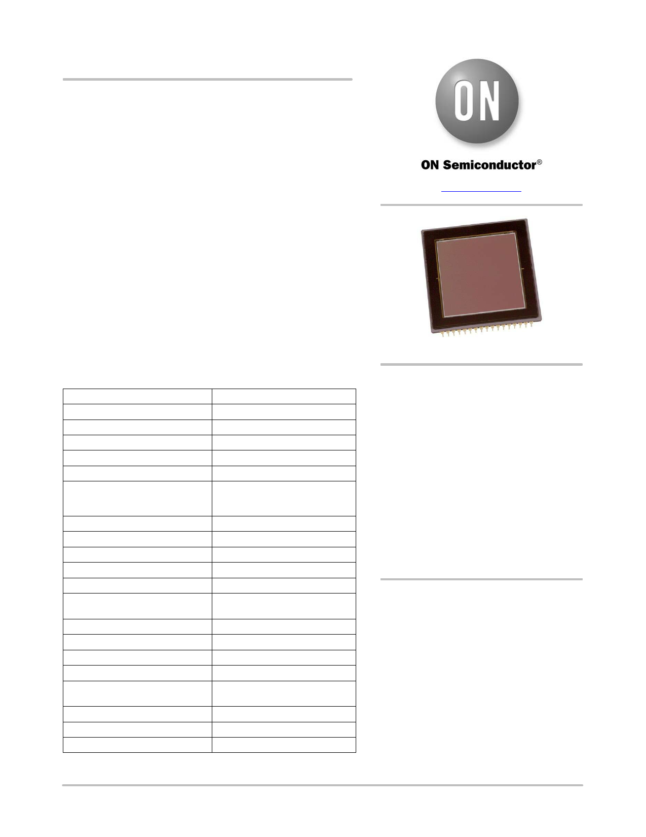
Figure 1. KAF−09000 CCD Image Sensor
Features
• TRUESENSE Transparent Gate Electrode
for High Sensitivity
• Large Pixel Size
• Large Image Area
• High Quantum Efficiency
• Low Noise Architecture
• Broad Dynamic Range
Applications
• Medical
• Scientific
ORDERING INFORMATION
See detailed ordering and shipping information on page 2 of
this data sheet.
Publication Order Number:
KAF−09000/D
1 page 
Output Load
KAF−09000
VDD = +15 V
Iout = 5 mA
VOUT
140 W
2N3904
or Equiv.
1 kW
0.1 μF
Buffered
Video
Output
Note: Component values may be revised based on operating conditions and other design considerations.
Figure 4. Recommended Output Structure Load Diagram
www.onsemi.com
5
5 Page 
KAF−09000
DEFECT DEFINITIONS
Operating Conditions
All cosmetic tests performed at approximately 25°C.
Table 6. SPECIFICATIONS
Classification
Standard Grade
Points
< 200
Clusters
< 20
Columns
< 10
Includes Dead Columns
yes
Point Defects
Dark: A pixel, which deviates by more than 6% from
neighboring pixels when illuminated to 70% of saturation
−or−
Bright: A Pixel with dark current > 3,000 e/pixel/sec at 25°C
Cluster Defect
A grouping of not more than 10 adjacent point defects
Cluster defects are separated by no less than 4 good pixels
in any direction
Column Defect
A grouping of more than 10 point defects along a single
column
−or−
A column containing a pixel with dark current
> 15,000 e/pixel/sec (bright column)
−or−
A column that does not meet the CTE specification for all
exposures less than the specified Max sat. signal level and
greater than 2 ke−
A pixel, which loses more than 250 e− under 2 ke−
illumination (trap defect)
Column defects are separated by no less than 4 good
columns. No multiple column defects (double or more) will
be permitted.
Column and cluster defects are separated by at least 4
good columns in the x direction.
www.onsemi.com
11
11 Page | ||
| Páginas | Total 21 Páginas | |
| PDF Descargar | [ Datasheet KAF-09000-ABA.PDF ] | |
Hoja de datos destacado
| Número de pieza | Descripción | Fabricantes |
| KAF-09000-ABA | CCD Image Sensor | ON Semiconductor |
| Número de pieza | Descripción | Fabricantes |
| SLA6805M | High Voltage 3 phase Motor Driver IC. |
Sanken |
| SDC1742 | 12- and 14-Bit Hybrid Synchro / Resolver-to-Digital Converters. |
Analog Devices |
|
DataSheet.es es una pagina web que funciona como un repositorio de manuales o hoja de datos de muchos de los productos más populares, |
| DataSheet.es | 2020 | Privacy Policy | Contacto | Buscar |