|
|
|
PDF XR28V384 Data sheet ( Hoja de datos )
| Número de pieza | XR28V384 | |
| Descripción | 3.3V QUAD LPC UART | |
| Fabricantes | Exar | |
| Logotipo | ||
Hay una vista previa y un enlace de descarga de XR28V384 (archivo pdf) en la parte inferior de esta página. Total 30 Páginas | ||
|
No Preview Available !
XR28V384
3.3V QUAD LPC UART WITH 128-BYTE FIFO
NOVEMBER 2013
REV. 1.0.0
GENERAL DESCRIPTION
The XR28V384 (V384) is a quad Universal
Asynchronous Receiver and Transmitter (UART) for
the Intel Low Pin Count (LPC) bus interface. This
device can replace or supplement a Super I/O device
to add additional serial ports to the system.
The V384 UARTs support any 16-bit I/O address
supported by the system. The register set is based on
the industry standard 16550 UART, so the V384
operates with the standard serial port drivers without
requiring a custom driver to be installed.
The 128 byte Transmit and Receive FIFOs reduce
CPU overhead and minimize the chance of buffer
overflow and data loss. In addition to the 16550
UART registers, there are also Configuration register
set where enhanced features such as the 9-bit
(multidrop) mode, IrDA mode and the Watchdog
Timer can be enabled.
The V384 is available in a 48-pin TQFP package.
APPLICATIONS
x Industrial and Embedded PCs
x Factory Automation and Process Controls
x Network Routers
x System Board Designs
FEATURES
x 128 Byte Transmit and Receive FIFO
x Compliant to LPC 1.1 Specifications
x -40°C to +85°C Industrial Temp Operation
x Watchdog Timer with WDTOUT# signal
x 4 Independent UART channels
■ Programmable I/O mapped base addresses
■ Data rates up to 3 Mbps
■ Selectable RX FIFO interrupt trigger levels
■ Auto RS-485 Half-Duplex Control mode
■ Programmable character lengths (5, 6, 7, 8)
with even, odd, or no parity
■ IrDA mode and separate IRTXA# and IRRXA#
pins for the first UART channel
■ 9-bit (Multidrop) mode
x External 24MHz/48MHz clock
x Single 3.3V Supply Voltage ( ±10% )
x 5V tolerant inputs
x 48-TQFP package (7mm x 7mm)
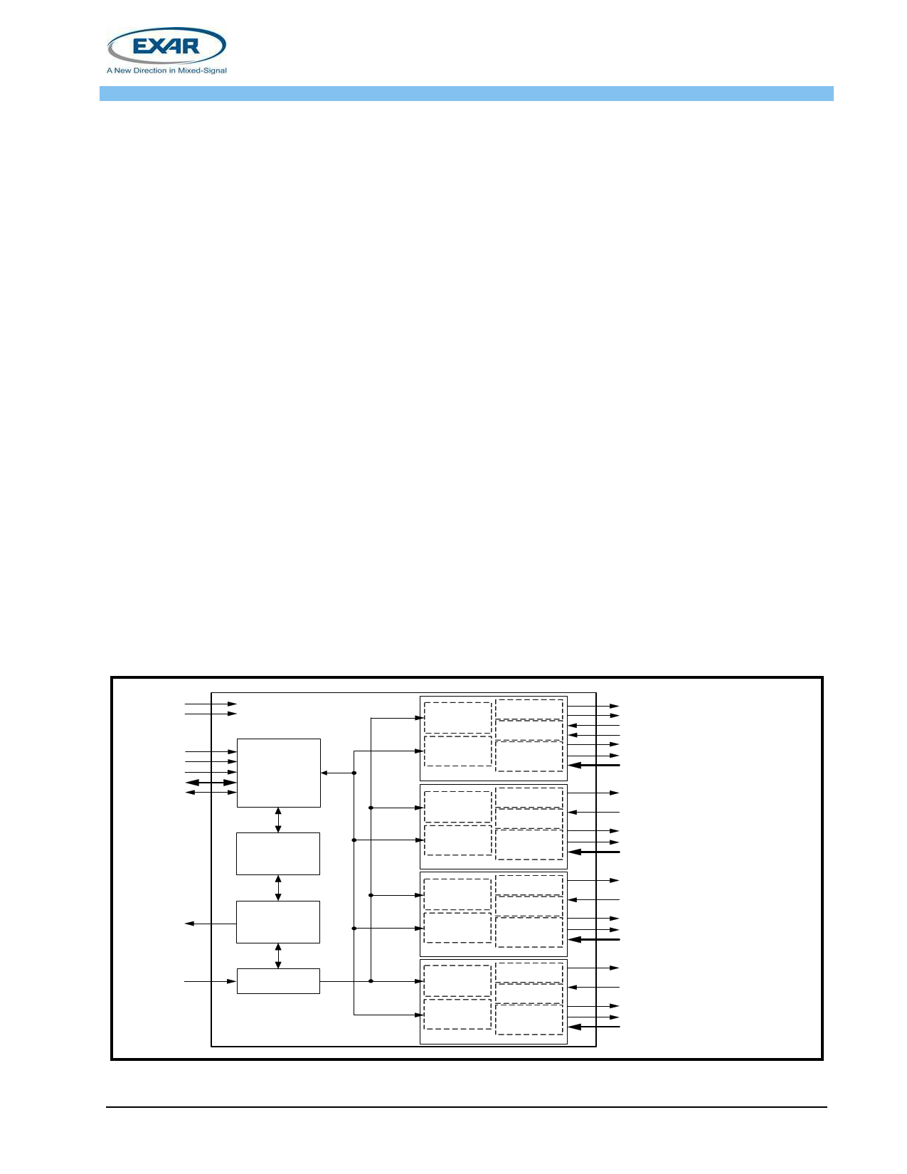
FIGURE 1. XR28V384 BLOCK DIAGRAM
VCC
GND
P C IR S T #
LCLK
LFR AM E
#
LA D [3:0]
S E R IR Q
W DTOUT
#
CLKI
N
3.3V ± 10%
LPC
Bus
In te rfa c e
G lo b a l
C o n fig u ra tio n
R e g iste rs
W atch
Dog
T im e r
C lo ck
D ivid e r
Baud
R ate
G enerator
S tatus and
C ontrol
R e g iste rs
T X F IF O
(IrD A E ncod er)
R X F IF O
(IrD A D ecoder)
M odem
IO s
UART Channel A
Baud
R ate
G enerator
S tatus and
C ontrol
R e g iste rs
T X F IF O
R X F IF O
M odem
IO s
UART Channel B
Baud
R ate
G enerator
S tatus and
C ontrol
R e g iste rs
T X F IF O
R X F IF O
M odem
IO s
UART Channel C
Baud
R ate
G enerator
S tatus and
C ontrol
R e g iste rs
T X F IF O
R X F IF O
M odem
IO s
UART Channel D
T X A /P S _3F 8_IR Q A
IR T X A #
RXA
IR R X A #
R T S A #/P S _C O N F _2E /R S 485
D T R A #/P S _3E 0_IR Q A
C T S A #, D S R A #, C D A #, R IA #
T X B /P S _2F 8_IR Q B
RXB
R T S B #/P S _C O N F _K E Y 1/R S 485
D T R B #/P S _2E 0_IR Q B
C T S B #, D S R B #, C D B #, R IB #
T X C /P S _3E 8_IR Q C
RXC
R T S C #/P S _C O N F _K E Y 0/R S 485
D T R C #/P S _W D T
C T S C #, D S R C #, C D C #, R IC #
T X D /P S _2E 8_IR Q D
RXD
R T S D #/R S 485
DTRD#
CTSD#, DSRD#, CDD#,
R ID #
Exar Corporation 48720 Kato Road, Fremont CA, 94538 • (510) 668-7000 • FAX (510) 668-7017 • www.exar.com
1 page 
XR28V384
REV. 1.0.0
Pin Description
3.3V QUAD LPC UART WITH 128-BYTE FIFO
NAME
48-TQFP
PIN#
TYPE
DESCRIPTION
RIB#
38
I
UART Channel B Ring-Indicator (active low) or general purpose input. This input
should be connected to VCC or GND when not used.
CTSA#
39
I
UART Channel A Clear-to-Send (active low) or general purpose input. This input
should be connected to VCC or GND when not used.
DSRA#
40
I
UART Channel A Data-Set-Ready (active low) or general purpose input. This
input should be connected to VCC or GND when not used.
RTSA# /
PS_CONF_2E/
RS485
41
UART Channel A Request-to-Send (active low) or general purpose output.
O This pin has an internal pull-up resistor and is sampled upon power-up or reset.
The registers can later be modified by the software. See Table 1 ’UART Power
On Configuration’.
DTRA# /
PS_3E0_IRQA
42
UART Channel A Data-Terminal-Ready (active low) or general purpose output.
This pin has an internal pull-up resistor and is sampled upon power-up or reset.
O This will determine the default register settings for UART Channel A. The regis-
ters can later be modified by the software. See Table 1 ’UART Power On Con-
figuration’.
RXA
43
I
UART Channel A Receive data.The receive data input must idle at logic 1 condi-
tion. This input should be connected to VCC or GND when not used.
TXA /
PS_3F8_IRQA
44
UART Channel A Transmit Data. The TXA signal will be a logic 1 during reset or
idle (no data). If it is not used, leave it unconnected.
O This pin has an internal pull-up resistor and is sampled upon power-up or reset.
This will determine the default register settings for UART Channel A. The regis-
ters can later be modified by the software. See Table 1 ’UART Power On Con-
figuration’.
CDA#
45
I
UART Channel A Carrier-Detect (active low) or general purpose input. This input
should be connected to VCC or GND when not used.
RIA#
46
I
UART Channel A Ring-Indicator (active low) or general purpose input. This input
should be connected to VCC or GND when not used.
IRRXA#
47
I
Infrared Receiver input. The infrared receive data input idles at logic 0. This input
should be connected to GND when not used.
IRTXA#
48
O
Infrared Transmitter output. The IRTXA# signal will be a logic 0 during reset or
idle (no data).
ANCILLARY SIGNALS
CLKIN
12 I Clock input 24 MHz or 48 MHz.
WDTOUT#
Active low watchdog timer output. This pin is open drain and needs a pull-up
2 O resistor if it is used. The registers can later be modified by the software. See
Table 1 ’UART Power On Configuration’.
POWER SIGNALS
VCC
11, 30 Pwr 3.3V ± 10% power supply.
GND
3, 29 Pwr Power supply common, ground.
Pin type: I=Input, O=Output, I/O= Input/output, Pwr=Power supply.
5
5 Page 
XR28V384
REV. 1.0.0
3.3V QUAD LPC UART WITH 128-BYTE FIFO
1.4.2 Transmitter
The transmitter section comprises of an 8-bit Transmit Shift Register (TSR) and up to 128 bytes of FIFO which
includes a byte-wide Transmit Holding Register (THR). TSR shifts out every data bit with the internal sampling
clock. The transmitter sends the start bit followed by the number of data bits, inserts the proper parity bit if
enabled, and adds the stop bit(s). The status of the THR and TSR are reported in the Line Status Register
(LSR bit-5 and bit-6).
1.4.2.1
Transmit Holding Register (THR) - Write Only
The transmit holding register is an 8-bit register providing a data interface to the host processor. The host
writes transmit data byte to the THR to be converted into a serial data stream including start bit, data bits, parity
bit and stop bit(s). The least significant bit (Bit-0) becomes first data bit to go out. The THR is the input register
to the transmit FIFO of up to 128 bytes when FIFO operation is enabled by FCR bit-0. Every time a write
operation is made to the THR, the FIFO data pointer is automatically bumped to the next sequential data
location.
1.4.2.2 Transmitter Operation in non-FIFO Mode
The host loads transmit data to THR one character at a time. The THR empty flag (LSR bit-5) is set when the
data byte is transferred to TSR. THR flag can generate a transmit empty interrupt (ISR bit-1) when it is enabled
by IER bit-1. The TSR flag (LSR bit-6) is set when TSR becomes completely empty.
FIGURE 3. TRANSMITTER OPERATION IN NON-FIFO MODE
Data
Byte
Transmit
Holding
Register
(THR)
THR Interrupt (ISR bit-1)
Enabled by IER bit-1
Clock
Transmit Shift Register (TSR)
ML
SS
BB
TXNOFIFO1
11
11 Page | ||
| Páginas | Total 30 Páginas | |
| PDF Descargar | [ Datasheet XR28V384.PDF ] | |
Hoja de datos destacado
| Número de pieza | Descripción | Fabricantes |
| XR28V382 | 3.3V DUAL LPC UART | Exar |
| XR28V384 | 3.3V QUAD LPC UART | Exar |
| Número de pieza | Descripción | Fabricantes |
| SLA6805M | High Voltage 3 phase Motor Driver IC. |
Sanken |
| SDC1742 | 12- and 14-Bit Hybrid Synchro / Resolver-to-Digital Converters. |
Analog Devices |
|
DataSheet.es es una pagina web que funciona como un repositorio de manuales o hoja de datos de muchos de los productos más populares, |
| DataSheet.es | 2020 | Privacy Policy | Contacto | Buscar |