|
|
|
PDF CDP68HC68S1 Data sheet ( Hoja de datos )
| Número de pieza | CDP68HC68S1 | |
| Descripción | Serial Multiplexed Bus Interface | |
| Fabricantes | Intersil Corporation | |
| Logotipo | ||
Hay una vista previa y un enlace de descarga de CDP68HC68S1 (archivo pdf) en la parte inferior de esta página. Total 14 Páginas | ||
|
No Preview Available !
CDP68HC68S1
April 1994
Serial Multiplexed Bus Interface
Features
• Differential Bus for Minimal EMl
• High Common Mode Noise Rejection
• Ideal for Twisted Pair Wiring
• Data Collision Detection
• Bus Arbitration
• Idle Detection
• Programmable Clock Divider
• Power-On Reset
Ordering Information
PART
NUMBER
CDP68HC68S1E
CDP68HC68S1M
TEMPERATURE
RANGE
PACKAGE
-40oC to +105oC 14 Lead PDIP
-40oC to +105oC 20 Lead SOIC (W)
Description
The CDP68HC6SS1 Serial Bus Interface Chip (SBlC) provides
a means of interfacing in a Small Area Network configuration,
various microcomputers (MCU’s) containing serial ports. Such
MCU’s include the family of 68HC05 microcontrollers. The SBlC
provides a connection from an MCU’s Serial Communication
Interface (asynchronous UART type interface) or Serial Periph-
eral Interface (synchronous) to a medium speed asynchronous
two wire differential signal bus designed to minimize electro-
magnetic interference. This two wire bus forms the network bus
to which all MCU’s are connected (through SBI chips). See Fig-
ure 1. Each MCU operates independently and may be added or
deleted from the bus with little or no impact on bus operation.
Such a bus is ideal for inter-microcomputer communication in
hazardous electrical environments such as automobiles, aircraft
or industrial control systems.
In addition to acting as bus arbitor and interface for microcom-
puter SCI port to differential bus communication, the
CDP68HC68S1 contains all the circuitry required to convert
and synchronize Non-Return-to-Zero (NRZ) 8-bit data received
on the differential bus and clock the data into a microcomputer’s
SPl port. Likewise, data to be sent by a microcomputer’s SPI
port is converted to asynchronous format by appending start
and stop bits before transmitting to other microcomputers.
Refer to the data sheet for the CDP68HCO5C4 for additional
information regarding CDP68HCO5 microcomputers and their
Serial Communications and Serial Peripheral Interfaces.
The CDP68HC68S1 is supplied in a 14 lead dual-in-line plastic
package (E suffix), and in a 20 lead small outline plastic pack-
age (M suffix).
Operating voltage ranges from 4V to 7V and operating temper-
ature ranges from -40oC to +105oC.
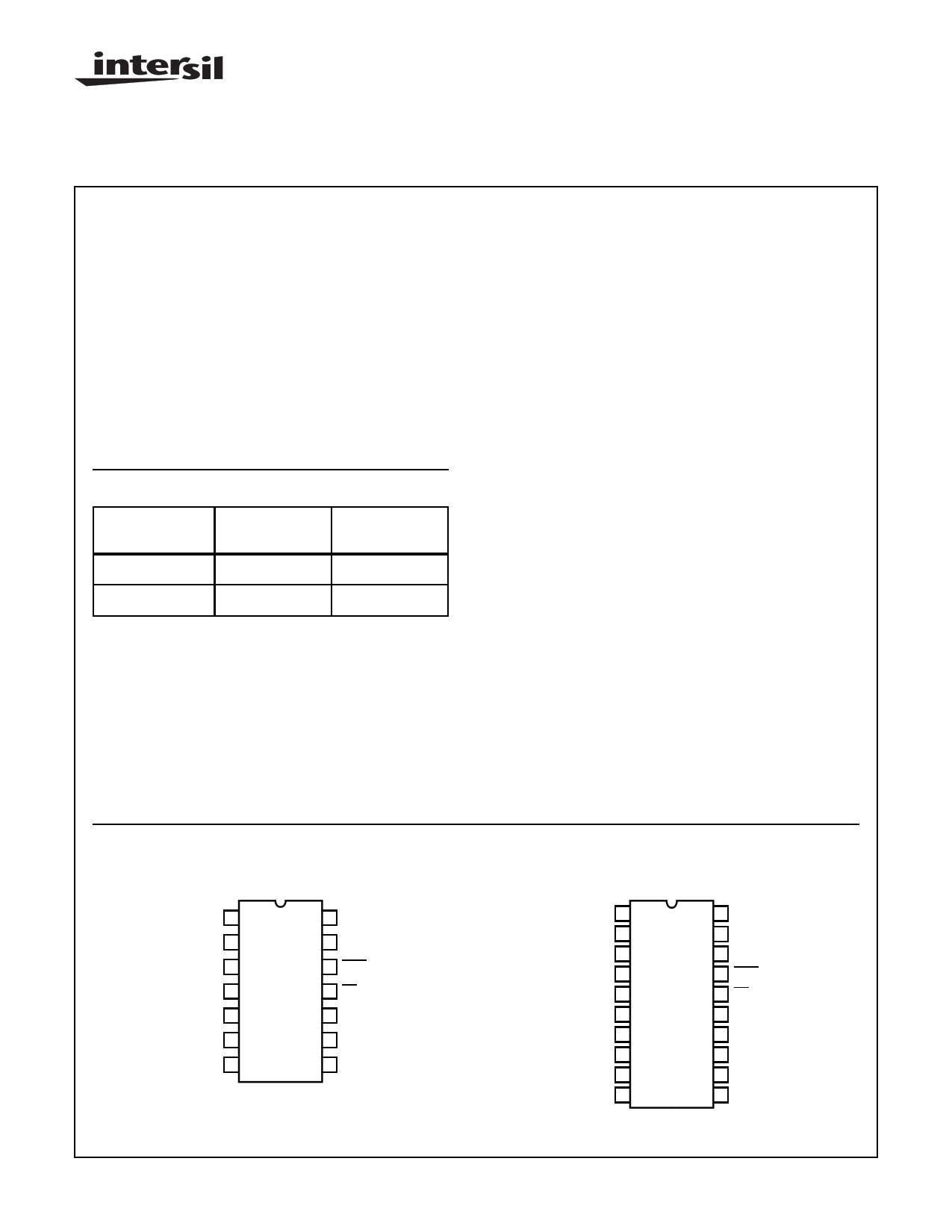
Pinouts
CD68HC68S1 (PDIP)
TOP VIEW
CLK 1
A2
B3
MODE 4
BUS+ 5
BUS- 6
VSS 7
14 VDD
13 CONTROL
12 IDLE
11 CS
10 SCK
9 REC
8 XMIT
CD68HC68S1 (SOIC)
TOP VIEW
CLK 1
A2
B3
MODE 4
NC 5
NC 6
BUS+ 7
NC 8
BUS- 9
VSS 10
20 VDD
19 CONTROL
18 NC
17 IDLE
16 CS
15 SCK
14 NC
13 NC
12 REC
11 XMIT
CAUTION: These devices are sensitive to electrostatic discharge; follow proper IC Handling Procedures.
407-727-9207 | Copyright © Intersil Corporation 1999
6-84
File Number 1918.3
1 page 
CDP68HC68S1
Functional Pin Description
PIN NUMBER SYMBOL
IN/OUT
DESCRIPTION
1
CLK
Input
This is the clock input that shall be divided by the SBIC (as described in Table 2) and used
as an internal synchronizing clock. The internal clock is then further divided by 128 to de-
termine baud rate, i.e. 128 internal clock periods constitute 1-bit length.
2, 3
A and B
Input
Programing inputs of the clock divider. These inputs are tied to +VDD or VSS depending
upon speed of external clock source. (See Table 2)
4
Mode
Input
This input shall be used in conjunction with CS input to define the mode of operation (see
Table 1). It may be permanently wired to +VDD or VSS or driven high or low by MCU I/O
lines.
5, 6
14, 7
8
9
10
BUS+
and BUS-
Input/Output
This is the two wire differential bus I/O used to transmit and receive data to and from the
differential bus. BUS+ is both responsive to, or driven positive by sourcing current from
an externally established bias point. This sourcing current matches the BUS- I/Os sinking
current. BUS- is both responsive to, or driven negative by sinking current from an exter-
nally established bias point. This sinking current matches the BUS+ I/Os sourcing current.
VDD and
VSS
XMIT
-
Input
Power and ground reference are supplied to the device via these pins. VDD is power and
VSS is ground.
In the SCI mode this data input shall come from the microcomputer standard NRZ asyn-
chronous communications output port (68HC05 SCI port pin TxD). In the SPI modes, it
shall come from the microcomputer’s synchronous output port (68HC05 SPI port pin
MOSl or MlSO).
REC
Output
In the SCI mode this data output shall be fed into the microcomputer asynchronous com-
munications input port (68HC05 SCI port pin RxD). In the SPI modes it shall be fed into
the microcomputer’s synchronous input port (6805 SP1 port pin MOSl or MISO).
SCK
Input/Output
In the SCI mode, this I/O is not required. In both SPI modes this pin is connected to the
68HC05’s SPI port SCK pin. In the normal SPl mode, the SBlC shall produce shift clock
pulses via this pin for synchronously shifting data into and out of the microcomputer. In
the Buffered SPl mode this pin is an input and the microcomputer shall generate the shift
clock pulses. Figure 3 shows the relationship between the serial clock signal and other
SBIC signals in the SPI mode.
11
CS
Input
This input shall be used in conjunction with the mode input and shall be used as a chip
select (see Table 1). It may be permanently wired to +VDD or VSS or driven high or low by
MCU I/O lines.
12
IDLE
Input/Output The microcomputer shall monitor this signal to determine the bus condition and also pull
this line low to generate a break. The IDLE signal goes low when the bus is idle (after
sensing an End of Message condition) and high when the bus is active. On reset, this pin
is set to a logic zero.
13 Control Input/Output The microcomputer shall monitor this I/O pin in the SPl mode to handle transmission and
reception of data. In the SCI and SPI modes, as an output, this pin will go low to indicate
that a data byte is currently active on the bus. In the Buffered SPI mode the control pin
indicates whether the user microcomputer has current access to the SBI chip’s internal 2
byte buffer (signified by a logic high on the control pin). In both SPI modes the control pin
is also effective as an input. In these modes the control pin is pulled low by the user mi-
crocomputer to initiate a transmit operation by the SBlC. The control pin is normally high
when the bus is inactive. On reset, this pin is set to a logic high.
All Intersil semiconductor products are manufactured, assembled and tested under ISO9000 quality systems certification.
Intersil products are sold by description only. Intersil Corporation reserves the right to make changes in circuit design and/or specifications at any time without
notice. Accordingly, the reader is cautioned to verify that data sheets are current before placing orders. Information furnished by Intersil is believed to be accurate
and reliable. However, no responsibility is assumed by Intersil or its subsidiaries for its use; nor for any infringements of patents or other rights of third parties which
may result from its use. No license is granted by implication or otherwise under any patent or patent rights of Intersil or its subsidiaries.
For information regarding Intersil Corporation and its products, see web site http://www.intersil.com
6-88
5 Page 
CDP68HC68S1
delay. Fortunately, SCl ports exhibit an inherent delay between
the loading of the transmit data buffer and the actual beginning
of the start bit appearing on the TXD pin. This delay, at 7812.5
Baud, can be as long as 256 SBl chip internal clock periods
and can be used to synchronize SCl users with SPI and Buff-
ered SPI users to ensure impartial bus arbitration. The delay for
a particular microcomputer must be determined by the user. If
this inherent delay is less than 256 clock periods, then the user
must delay the loading of the first byte enough to ensure that
the total delay including the inherent delay of the SCl port is 256
clock periods.
Framing Errors
While in the SCl mode, the SBI chip is capable of detecting
incoming framing errors. It will do this even though the
incoming signal is also echoed to the user microcomputer,
which should also detect the framing error via its’ UART.
When a framing error is detected by the SBl chip, the gener-
ation of the SCK pulses is terminated until and End Of Mes-
sage is detected.
The SPI Mode Hardware
MCU
TxD
RxD
PAO
SBIC
XMIT BUS+
REC
IDLE
BUS-
MODE CS
DIFFERENTIAL
BUS
+VDD
FIGURE 9. USING THE SCI MODE
Monitoring the IDLE Pin
The user microcomputer must monitor the IDLE pin on the SBlC
chip in order to determine when a message ends, when the next
received byte is a Msg ID byte, and when to attempt arbitration
if the user microcomputer has a message to transmit.
The Master Out Slave In, (MOSl), and Master In Slave Out,
(MISO), pins on the user microcomputer are connected to
the REC and XMlT pins of the SBl chip, respectively, as
shown in Figure 10. The SCK pins on the user microcom-
puter and the SBl chip are connected together. Synchroniza-
tion of data transferred between the user microcomputer and
the SBl chip is done by using the SCK signal provided by the
SBl chip.
In the SPl mode of operation the SBl chip should always be
properly mode selected. This may be accomplished either
by a user microcomputer output signal or by permanent wir-
ing in order to guarantee that the SBl chip will always be
able to receive messages from other microcomputers on the
bus, which may happen at random. To select the SPl mode,
set the MODE pin to a logic l and the CS pin to a logic 0.
The user microcomputer must be able to both detect when
the IDLE signal goes from high to low and sense at other
times whether it is either high or low. Detecting the change
from high to low is necessary in order to know exactly when
the bus goes idle. An MCU can then begin bus arbitration by
attempting to transmit. Being able to sense the level of IDLE
is necessary in order to be able to start transmitting a mes-
sage sometime after IDLE has gone low but no other user on
the bus has had a message to transmit for a length of time.
Instead of polling the IDLE pin via an MCU input pin, the
user may wish to conserve CPU time by using interrupts to
monitor bus activity. The user microcomputer’s external
interrupt pin (IRQ) can be used to edge detect the IDLE pin
for high to low transitions.
Using 68HC05 SCl Port Flags
During message reception, the 68HC05 SCl port receive
data register full flag (RDRF), and optionally its associated
interrupt, can be used by the user microcomputer to deter-
mine when to unload the next received byte.
The user may wish to ignore the RDRF flag and disable the
RDRF interrupt during reception of an unwanted message.
In this case the user can merely wait for the IDLE pin to go
low before attempting any further actions.
The normally available transmit data register empty flag
(TDRE) can be used to determine when to load the next byte
to be transmitted onto the bus. If there are no more bytes to
be transmitted, then consider the last message as having
been transmitted, and generate an End Of Message (EOM)
(i.e. transmit a logic 1 for 10 contiguous bit times by creating
a software delay).
MCU
MISO
MOSI
SCK
SS
PAO
PA1
SBIC
XMIT BUS+
REC
SCK
BUS-
VSS
IDLE
CONTROL
DIFFERENTIAL
BUS
MODE CS
+VDD
VSS
FIGURE 10. USING THE SPI MODE
The user microcomputer should configure its SPl port for
slave mode operation with SCK positive polarity and data
transfer on SCK leading edge (i.e. CPOL = 0, CPHA = 1, for
68HC05 microcomputers). 8-bit data transfers between the
user microcomputer and the SBl chip occur at differential
bus transfer speed.
In the SPI mode, the user microcomputer operates in the
slave mode and the SBl chip operates as the master. The
SS pin on the user microcomputer must be wired low or
forced low whenever the SBl chip has incoming data. It may
be useful to connect the CONTROL pin of the SBl chip to the
Slave Select (SS) pin of the 68HC05 microcomputer. The
SBl chip will then control the user microcomputer’s SPI port.
The user microcomputer can request transmission of data
onto the bus by the SBl chip by loading data into its SPl data
register and then pulling the SBlC’s CONTROL pin low (for
at least 1µs). However, it must do so before the SBl chip has
begun to receive data from another MCU.
6-94
11 Page | ||
| Páginas | Total 14 Páginas | |
| PDF Descargar | [ Datasheet CDP68HC68S1.PDF ] | |
Hoja de datos destacado
| Número de pieza | Descripción | Fabricantes |
| CDP68HC68S1 | Serial Multiplexed Bus Interface | Intersil Corporation |
| CDP68HC68S1E | Serial Multiplexed Bus Interface | Intersil Corporation |
| CDP68HC68S1M | Serial Multiplexed Bus Interface | Intersil Corporation |
| Número de pieza | Descripción | Fabricantes |
| SLA6805M | High Voltage 3 phase Motor Driver IC. |
Sanken |
| SDC1742 | 12- and 14-Bit Hybrid Synchro / Resolver-to-Digital Converters. |
Analog Devices |
|
DataSheet.es es una pagina web que funciona como un repositorio de manuales o hoja de datos de muchos de los productos más populares, |
| DataSheet.es | 2020 | Privacy Policy | Contacto | Buscar |