|
|
PDF CDP6402C Data sheet ( Hoja de datos )
| Número de pieza | CDP6402C | |
| Descripción | CMOS Universal Asynchronous Receiver/Transmitter (UART) | |
| Fabricantes | Harris Corporation | |
| Logotipo |  |
|
Hay una vista previa y un enlace de descarga de CDP6402C (archivo pdf) en la parte inferior de esta página. Total 12 Páginas | ||
|
No Preview Available !
SEMICONDUCTOR
August 1996
CDP6402,
CDP6402C
CMOS Universal Asynchronous
Receiver/Transmitter (UART)
Features
• Low Power CMOS Circuitry. . . . . . . . . . 7.5mW (Typ) at
3.2MHz (Max Freq.) at VDD = 5V
• Baud Rate
- DC to 200K Bits/s (Max) at. . . . . . . . . . . . . . 5V, 85oC
- DC to 400K Bits/s (Max) at. . . . . . . . . . . . . . 10V, 85oC
• 4V to 10.5 Operation
• Automatic Data Formatting and Status Generation
• Fully Programmable with Externally Selectable Word
Length (5 - 8 Bits), Parity Inhibit, Even/Odd Parity, and
1, 1-1/2, or 2 Stop Bits
• Operating Temperature Range
- CDP6402D, CD . . . . . . . . . . . . . . . . . -55oC to +125oC
- CDP6402E, CE . . . . . . . . . . . . . . . . . . -40oC to +85oC
• Replaces Industry Type IM6402 and Compatible with
HD6402
Ordering Information
PACK-
AGE
PDIP
Burn-In
SBDIP
Burn-In
5V/200K
TEMP. RANGE BAUD
-40oC to +85oC CDP6402CE
10V/400K
BAUD
CDP6402E
CDP6402CEX
-
-40oC to +85oC CDP6402CD CDP6402D
CDP6402CDX CDP6402DX
PKG.
NO.
E40.6
D40.6
Description
The CDP6402 and CDP6402C are silicon gate CMOS
Universal Asynchronous Receiver/Transmitter (UART)
circuits for interfacing computers or microprocessors to
asynchronous serial data channels. They are designed to
provide the necessary formatting and control for interfacing
between serial and parallel data channels. The receiver
converts serial start, data, parity, and stop bits to parallel
data verifying proper code transmission, parity and stop bits.
The transmitter converts parallel data into serial form and
automatically adds start parity and stop bits.
The data word can be 5, 6, 7 or 8 bits in length. Parity may
be odd, even or inhibited. Stop bits can be 1, 1-1/2, or 2
(when transmitting 5-bit code).
The CDP6402 and CDP6402C can be used in a wide range
of applications including modems, printers, peripherals,
video terminals, remote data acquisition systems, and serial
data links for distributed processing systems.
The CDP6402 and CDP6402C are functionally identical.
They differ in that the CDP6402 has a recommended
operating voltage range of 4V to 10.5V, and the CDP6402C
has a recommended operating voltage range of 4V to 6.5V.
Pinout
(40 LEAD PDIP, SBDIP)
TOP VIEW
VDD 1
NC 2
GND 3
RRD 4
RBR8 5
RBR7 6
RBR6 7
RBR5 8
RBR4 9
RBR3 10
RBR2 11
RBR1 12
PE 13
FE 14
OE 15
SFD 16
RRC 17
DRR 18
DR 19
RRI 20
40 TRC
39 EPE
38 CLS1
37 CLS2
36 SBS
35 PI
34 CRL
33 TBR8
32 TBR7
31 TBR6
30 TBR5
29 TBR4
28 TBR3
27 TBR2
26 TBR1
25 TRO
24 TRE
23 TBRL
22 TBRE
21 MR
CAUTION: These devices are sensitive to electrostatic discharge. Users should follow proper IC Handling Procedures.
Copyright © Harris Corporation 1996
5-74
File Number 1328.2
1 page 
CDP6402, CDP6402C
Description of Operation
Initialization and Controls
A positive pulse on the MASTER RESET (MR) input resets
the control, status, and receiver buffer registers, and sets the
serial output (TRO) High. Timing is generated from the clock
inputs RRC and TRC at a frequency equal to 16 times the
serial data bit rate. The RRC and TRC inputs may be driven
by a common clock, or may be driven independently by two
different clocks. The CONTROL REGISTER LOAD (CRL)
input is strobed to load control bits for PARITY INHIBIT (PI),
EVEN PARITY ENABLE (EPE), STOP BIT SELECTS (SBS),
and CHARACTER LENGTH SELECTS (CLS1 and CLS2).
These inputs may be hand wired to VSS or VDD with CRL to
VDD. When the initialization is completed, the UART is ready
for receiver and/or transmitter operations.
Transmitter Operation
The transmitter section accepts parallel data, formats it, and
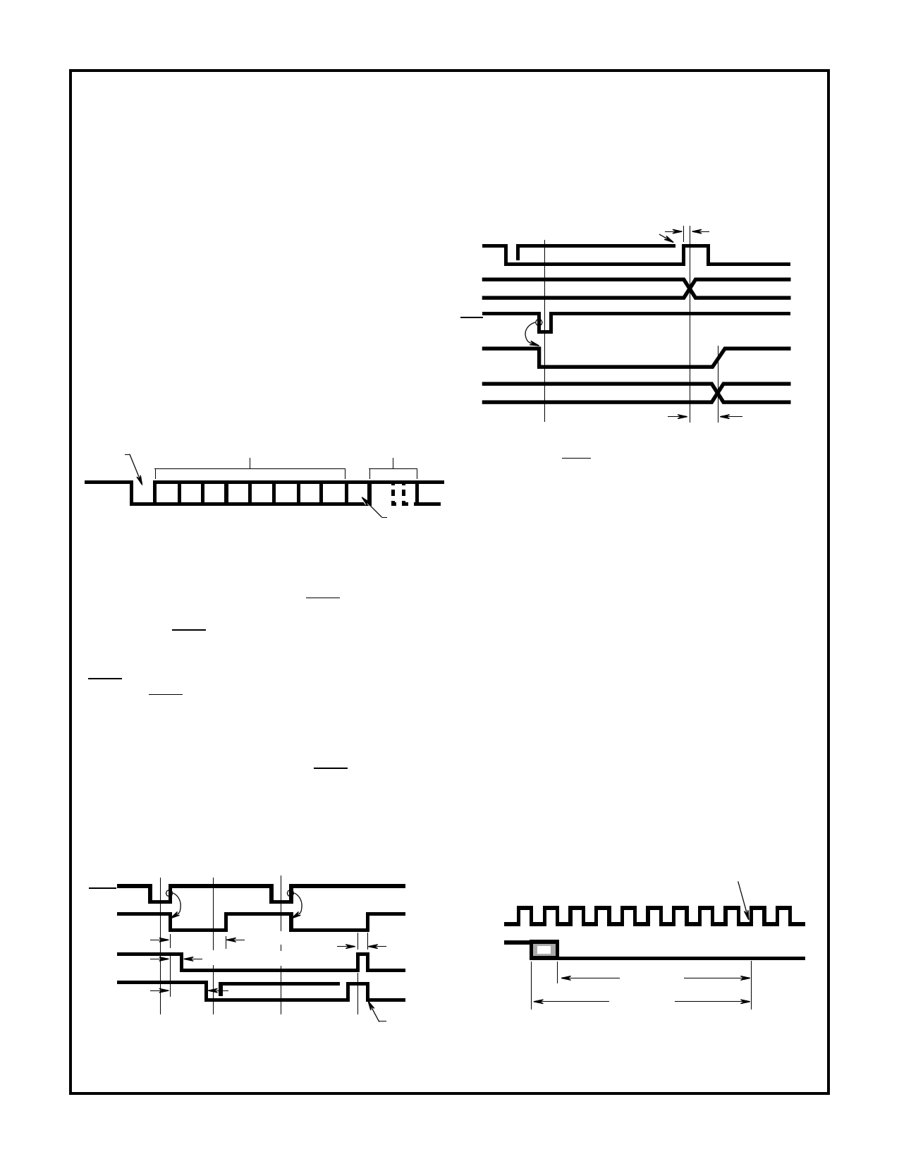
transmits it in serial form (Figure 2) on the TRO terminal.
START
BIT
5 - 8 DATA BITS
1, 1-1/2 OR
2 STOP BITS
LSB MSB †
† IF ENABLED
FIGURE 2. SERIAL DATA FORMAT
PARITY
Transmitter timing is shown in Figure 3. (A) Data is loaded
into the transmitter buffer register from the inputs TBR1
through TBR8 by a logic low on the TBRL input. Valid data
must be present at least tDT prior to, and tTD following, the
rising edge of TBRL. If words less than 8-bits are used, only
the least significant bits are used. The character is right justi-
fied into the least significant bit, TBR1. (B) The rising edge of
TBRL clears TBRE. 1/2 to 11/2 cycles later, depending on
when the TBRL pulse occurs with respect to TRC, data is
transferred to the transmitter register and TRE is cleared.
TBRE is set to a logic High one cycle after that.
Output data is clocked by TRC. The clock rate is 16 times
the data rate. (C) A second pulse on TBRL loads data into
the transmitter buffer register. Data transfer to the transmitter
register is delayed until transmission of the current character
is complete. (D) Data is automatically transferred to the
transmitter register and transmission of that character
begins.
TBRL
TBRE
TRE
1-1/2 TO 2-1/2 CYCLES
1/2 TO 1-1/2 CYCLES
1/2
CLOCK
TRO
1 TO 2 CYCLES DATA
AB
C
END OF
D LAST
STOP BIT
FIGURE 3. TRANSMITTER TIMING WAVEFORMS
Receiver Operation
Data is received in serial form at the RRl input. When no
data is being received, RRI input must remain high. The data
is clocked through the RRC. The clock rate is 16 times the
data rate. Receiver timing is shown in Figure 4.
BEGINNING OF FIRST STOP BIT
RRI
8 1/2 TO 9 1/2
CLOCK CYCLES
RBRI-8, OE
DRR
DR
FE, PE
1/2 CLOCK
A B C CYCLES
FIGURE 4. RECEIVER TIMING WAVEFORMS
(A) A low level on DRR clears the DR line. (B) During the first
stop bit data is transferred from the receiver register to the
RB Register. If the word is less than 8 bits, the unused most
significant bits will be a logic low. The output character is
right justified to the least significant bit RBR1. A logic high on
OE indicates overruns. An overrun occurs when DR has not
been cleared before the present character was transferred to
the RBR. (C) 1/2 clock cycle later DR is set to a logic high
and FE is evaluated. A logic high on FE indicates an invalid
stop bit was received. A logic high on PE indicates a parity
error.
Start Bit Detection
The receiver uses a 16X clock for timing (Figure 5). The start
bit could have occurred as much as one clock cycle before it
was detected, as indicated by the shaded portion. The cen-
ter of the start bit is defined as clock count 7 1/2. If the
receiver clock is a symmetrical square wave, the center of
the start bit will be located within ±1/2 clock cycle ±1/32 bit or
±3.125%. The receiver begins searching for the next start bit
at 9 clocks into the first stop bit.
COUNT 7 1/2
DEFINED CENTER
OF START BIT
CLOCK
RRI
INPUT
A
START
7 1/2 CLOCK
CYCLES
8 1/2 CLOCK
CYCLES
FIGURE 5. START BIT TIMING WAVEFORMS
5-78
5 Page 
CDP6402, CDP6402C
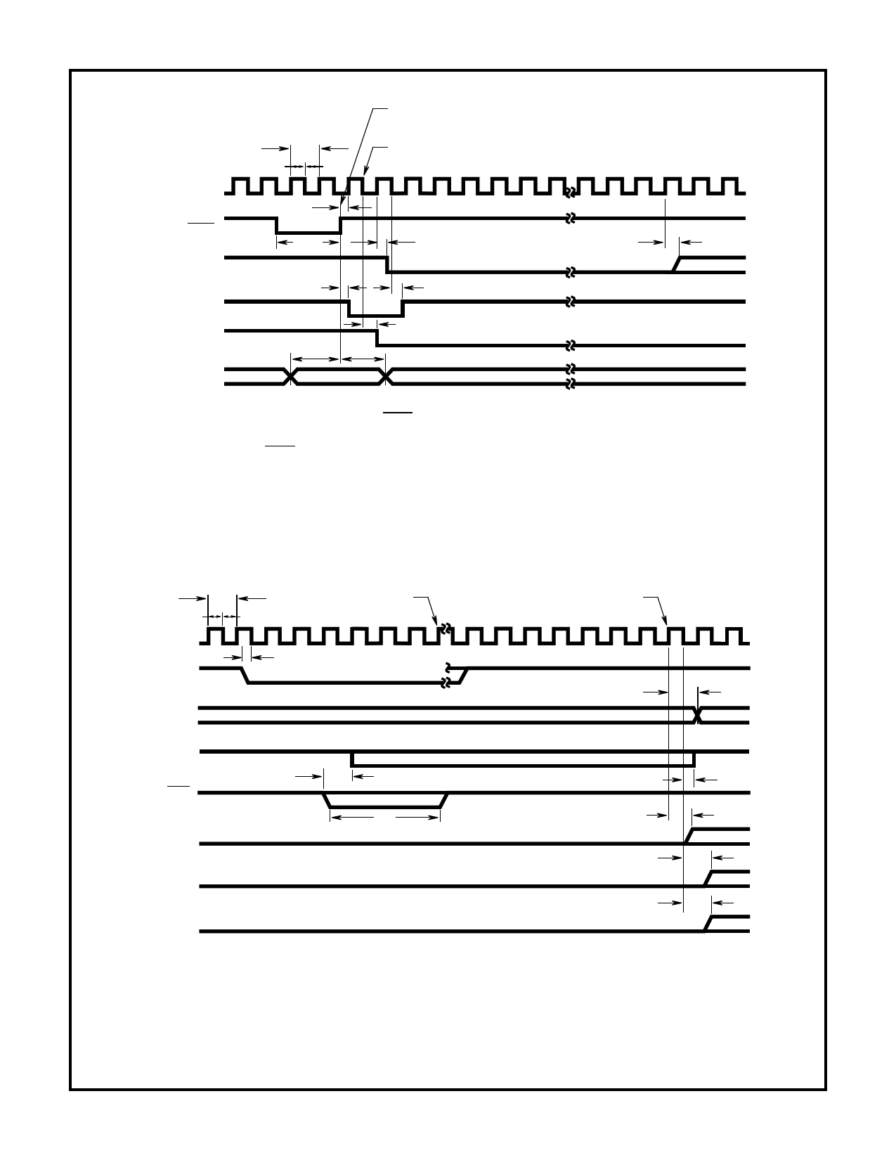
TRC
tCC
tCH tCL
tTHC
TRANSMITTER BUFFER
REGISTER LOADED
(NOTE 1)
TRANSMITTER SHIFT
REGISTER LOADED
(NOTE 2)
12 34 56
7 14 15 16 1 2
3
TBRL
tTHTH
tCD
tCD
TRO
tTTHR
tCT
1ST DATA BIT
TBRE
TRE
T BUS 0
T BUS 7
tDT tDT
DATA
tTTS
NOTES:
1. The holding register is loaded on the trailing edge of TBRL.
2. The transmitter shift register, if empty , is loaded on the first high-to-low transition of the clock which occurs at least 1/2 clock period +
tTHC after the trailing edge of TBRL and transmission of a start bit occurs 1/2 clock period + tCD later.
FIGURE 7. TRANSMITTER TIMING WAVEFORMS
tCC
tCH tCL
CLOCK 7 1/2
SAMPLE
CLOCK 7 1/2 LOAD
HOLDING REGISTER
RRC
tDC
(NOTE 1)
RRI
R BUS 0 -
R BUS 7
1 2 3 4 5 6 7 16 1 2 3 4 5 6 7 8 9
START BIT PARITY
STOP BIT 1
tCDV
DATA
DR
DRR
OE
(NOTE 2)
PE
FE
tDDA
tDD
tCOE
tCPE
tCFE
tCDA
NOTES:
1. If a start bit occurs at a time less than tDC before a high-to-low transition of the clock, the start bit may not be recognized until the next
high-to-low transition of the clock. The start bit may be completely asynchronous with the clock.
2. If a pending DA has not been cleared by a read of the receiver holding register by the time a new word is loaded into the receiver holding
register, the OE signal will come true..
FIGURE 8. RECEIVER TIMING WAVEFORMS
5-84
11 Page | ||
| Páginas | Total 12 Páginas | |
| PDF Descargar | [ Datasheet CDP6402C.PDF ] | |
Hoja de datos destacado
| Número de pieza | Descripción | Fabricantes |
| CDP6402 | CMOS Universal Asynchronous Receiver/Transmitter | GE |
| CDP6402 | CMOS Universal Asynchronous Receiver/Transmitter (UART) | Harris Corporation |
| CDP6402C | CMOS Universal Asynchronous Receiver/Transmitter | GE |
| CDP6402C | CMOS Universal Asynchronous Receiver/Transmitter (UART) | Harris Corporation |
| Número de pieza | Descripción | Fabricantes |
| SLA6805M | High Voltage 3 phase Motor Driver IC. |
Sanken |
| SDC1742 | 12- and 14-Bit Hybrid Synchro / Resolver-to-Digital Converters. |
Analog Devices |
|
DataSheet.es es una pagina web que funciona como un repositorio de manuales o hoja de datos de muchos de los productos más populares, |
| DataSheet.es | 2020 | Privacy Policy | Contacto | Buscar |
