|
|
|
PDF TL431A Data sheet ( Hoja de datos )
| Número de pieza | TL431A | |
| Descripción | Programmable Precision References | |
| Fabricantes | ON Semiconductor | |
| Logotipo | ||
Hay una vista previa y un enlace de descarga de TL431A (archivo pdf) en la parte inferior de esta página. Total 18 Páginas | ||
|
No Preview Available !
TL431A, B Series,
NCV431A, B Series,
SCV431A
Programmable
Precision References
The TL431A, B integrated circuits are three−terminal
programmable shunt regulator diodes. These monolithic IC voltage
references operate as a low temperature coefficient zener which is
programmable from Vref to 36 V with two external resistors. These
devices exhibit a wide operating current range of 1.0 mA to 100 mA
with a typical dynamic impedance of 0.22 W. The characteristics of
these references make them excellent replacements for zener diodes in
many applications such as digital voltmeters, power supplies, and op
amp circuitry. The 2.5 V reference makes it convenient to obtain a
stable reference from 5.0 V logic supplies, and since the TL431A, B
operates as a shunt regulator, it can be used as either a positive or
negative voltage reference.
Features
• Programmable Output Voltage to 36 V
• Voltage Reference Tolerance: ±0.4%, Typ @ 25°C (TL431B)
• Low Dynamic Output Impedance, 0.22 W Typical
• Sink Current Capability of 1.0 mA to 100 mA
• Equivalent Full−Range Temperature Coefficient of 50 ppm/°C Typical
• Temperature Compensated for Operation over Full Rated Operating
Temperature Range
• Low Output Noise Voltage
• NCV/SCV Prefixes for Automotive and Other Applications
Requiring Unique Site and Control Change Requirements;
AEC−Q100 Qualified and PPAP Capable
• These Devices are Pb−Free, Halogen Free/BFR Free and are RoHS
Compliant
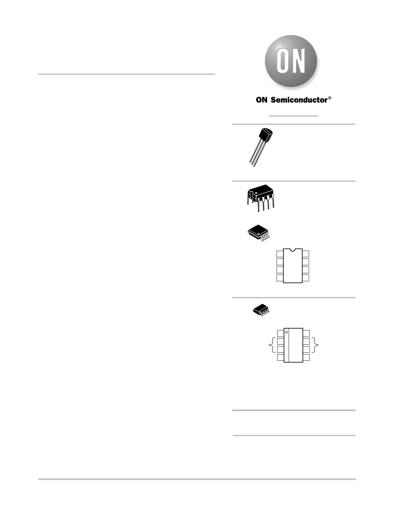
www.onsemi.com
TO−92 (TO−226)
LP SUFFIX
CASE 29
Pin 1. Reference
1 23
2. Anode
3. Cathode
8
1
PDIP−8
P SUFFIX
CASE 626
Micro8E
DM SUFFIX
CASE 846A
Cathode 1
N/C 2
N/C 3
N/C 4
8 Reference
7 N/C
6 Anode
5 N/C
(Top View)
8
1
SOIC−8
D SUFFIX
CASE 751
Cathode 1
Anode
2
3
N/C 4
8 Reference
7
Anode
6
5 N/C
(Top View)
This is an internally modified SOIC−8 package. Pins 2, 3, 6 and
7 are electrically common to the die attach flag. This internal
lead frame modification increases power dissipation capability
when appropriately mounted on a printed circuit board. This
modified package conforms to all external dimensions of the
standard SOIC−8 package.
ORDERING INFORMATION
See detailed ordering and shipping information on page 13 of
this data sheet.
DEVICE MARKING INFORMATION
See general marking information in the device marking
section on page 14 of this data sheet.
© Semiconductor Components Industries, LLC, 2016
March, 2016 − Rev. 38
1
Publication Order Number:
TL431/D
1 page 
TL431A, B Series, NCV431A, B Series, SCV431A
Input IK VKA
Vref
Figure 1. Test Circuit for VKA = Vref
Input VKA
R1 Iref
IK
Input VKA
Ioff
ǒ ǓR2 VKA + Vref 1 ) RR12 ) Iref S R1
Vref
Figure 2. Test Circuit for VKA > Vref
Figure 3. Test Circuit for Ioff
150
VKA = Vref
TA = 25°C
100 Input
VKA
IK
50
0
-50
-100
-2.0
-1.0 0 1.0 2.0
VKA, CATHODE VOLTAGE (V)
Figure 4. Cathode Current versus
Cathode Voltage
3.0
800
VKA = Vref
TA = 25°C
600 Input
IKVKA
400
IMin
200
0
-20-01.0
0 1.0 2.0
VKA, CATHODE VOLTAGE (V)
Figure 5. Cathode Current versus
Cathode Voltage
3.0
2600
Input
2580
2560 Vref
2540
VKA
IK VKA = Vref
IK = 10 mA
Vref Max = 2550 mV
2520
2500 Vref Typ = 2495 mV
2480
2460
2440 Vref Min = 2440 mV
2420
2400
-55 -25 0 25 50 75 100 125
TA, AMBIENT TEMPERATURE (°C)
Figure 6. Reference Input Voltage versus
Ambient Temperature
3.0
2.5
2.0
1.5
IK = 10 mA
1.0 Input
10k Iref
VKA
IK
0.5
0-55 -25 0 25 50 75 100 125
TA, AMBIENT TEMPERATURE (°C)
Figure 7. Reference Input Current versus
Ambient Temperature
www.onsemi.com
5
5 Page 
TL431A, B Series, NCV431A, B Series, SCV431A
APPLICATIONS INFORMATION
The TL431 is a programmable precision reference which
is used in a variety of ways. It serves as a reference voltage
in circuits where a non−standard reference voltage is
needed. Other uses include feedback control for driving an
optocoupler in power supplies, voltage monitor, constant
current source, constant current sink and series pass
regulator. In each of these applications, it is critical to
maintain stability of the device at various operating currents
and load capacitances. In some cases the circuit designer can
estimate the stabilization capacitance from the stability
boundary conditions curve provided in Figure 15. However,
these typical curves only provide stability information at
specific cathode voltages and at a specific load condition.
Additional information is needed to determine the
capacitance needed to optimize phase margin or allow for
process variation.
A simplified model of the TL431 is shown in Figure 31.
When tested for stability boundaries, the load resistance is
150 W. The model reference input consists of an input
transistor and a dc emitter resistance connected to the device
anode. A dependent current source, Gm, develops a current
whose amplitude is determined by the difference between
the 1.78 V internal reference voltage source and the input
transistor emitter voltage. A portion of Gm flows through
compensation capacitance, CP2. The voltage across CP2
drives the output dependent current source, Go, which is
connected across the device cathode and anode.
Model component values are:
Vref = 1.78 V
Gm = 0.3 + 2.7 exp (−IC/26 mA)
where IC is the device cathode current and Gm is in mhos
Go = 1.25 (Vcp2) mmhos.
Resistor and capacitor typical values are shown on the
model. Process tolerances are ± 20% for resistors, ±10% for
capacitors, and ±40% for transconductances.
An examination of the device model reveals the location
of circuit poles and zeroes:
P1
+
2p
1
RGM
CP1
+
2p
*
1.0
1
M
*
20
pF
+
7.96
kHz
P2
+
2p
1
RP2CP2
+
2p
*
10
1
M*
0.265
pF
+
60
kHz
Z1
+
2p
1
RZ1CP1
+
2p
*
1
15.9 k
*
20
pF
+
500
kHz
In addition, there is an external circuit pole defined by the
load:
PL
+
2p
1
RLCL
Also, the transfer dc voltage gain of the TL431 is:
Example 1:
G + GMRGMGoRL
IC + 10 mA, RL+ 230 W, CL+ 0. Define the transfer gain.
The DC gain is:
G + GMRGMGoRL +
(2.138)(1.0 M)(1.25 m)(230) + 615 + 56 dB
Loop
gain +
G
8.25 k
8.25 k ) 15 k
+
218 +
47
dB
The resulting transfer function Bode plot is shown in
Figure 32. The asymptotic plot may be expressed as the
following equation:
ǒ Ǔ1
)
jf
500 kHz
ǒ Ǔǒ ǓAv + 615
1
)
jf
8.0 kHz
1
)
60
jf
kHz
The Bode plot shows a unity gain crossover frequency of
approximately 600 kHz. The phase margin, calculated from
the equation, would be 55.9 degrees. This model matches the
Open−Loop Bode Plot of Figure 12. The total loop would
have a unity gain frequency of about 300 kHz with a phase
margin of about 44 degrees.
www.onsemi.com
11
11 Page | ||
| Páginas | Total 18 Páginas | |
| PDF Descargar | [ Datasheet TL431A.PDF ] | |
Hoja de datos destacado
| Número de pieza | Descripción | Fabricantes |
| TL431 | ADJUSTABLE PRECISION SHUNT REGULATOR | Diodes |
| TL431 | PROGRAMMABLE PRECISION REFERENCES | Motorola Semiconductors |
| TL431 | PROGRAMMABLE PRECISION REFERENCES | ON Semiconductor |
| TL431 | PROGRAMMABLE VOLTAGE REFERENCE | STMicroelectronics |
| Número de pieza | Descripción | Fabricantes |
| SLA6805M | High Voltage 3 phase Motor Driver IC. |
Sanken |
| SDC1742 | 12- and 14-Bit Hybrid Synchro / Resolver-to-Digital Converters. |
Analog Devices |
|
DataSheet.es es una pagina web que funciona como un repositorio de manuales o hoja de datos de muchos de los productos más populares, |
| DataSheet.es | 2020 | Privacy Policy | Contacto | Buscar |