|
|
|
PDF F2933 Data sheet ( Hoja de datos )
| Número de pieza | F2933 | |
| Descripción | High Reliability SP2T RF Switch | |
| Fabricantes | Integrated Device Technology | |
| Logotipo | ||
Hay una vista previa y un enlace de descarga de F2933 (archivo pdf) en la parte inferior de esta página. Total 19 Páginas | ||
|
No Preview Available !
High Reliability SP2T RF Switch
GENERAL DESCRIPTION
The F2933 is a high reliability, low insertion loss, 50 Ω
SP2T absorptive RF switch designed for a multitude of
wireless and other RF applications. This device covers
a broad frequency range from 50 MHz to 8000 MHz.
In addition to providing low insertion loss, the F2933
also delivers high linearity and high isolation
performance while providing a 50 Ω termination to the
unused RF input port.
The F2933 uses a single positive supply voltage of
2.7 V to 5.5 V supporting three states using either
3.3 V or 1.8 V control logic.
COMPETITIVE ADVANTAGE
The F2933 provides the following advantages
Insertion Loss = 0.79 dB*
RFX to RFC Isolation = 67 dB*
IIP3 = +64 dBm*
Active Port Operating Power Handling = 34 dBm
Term Port Operating Power Handling = 27 dBm
Extended Temperature Range = -40°C to 105°C
* 2 GHZ
APPLICATIONS
• Base Station 2G, 3G, 4G
• Portable Wireless
• Repeaters and E911 systems
• Digital Pre-Distortion
• Point to Point Infrastructure
• Public Safety Infrastructure
• WIMAX Receivers and Transmitters
• Military Systems, JTRS radios
• RFID handheld and portable readers
• Test / ATE Equipment
F2933
Datasheet
50 MHz to 8000 MHz
FEATURES
• High Isolation:
o 70 dB @ 1 GHz
o 67 dB @ 2 GHz
o 65 dB @ 3 GHz
o 66 dB @ 4 GHz
• High Linearity:
o IIP2 of 111 dBm
o IIP3 of 64 dBm @ 2 GHz
• Wide Single Positive Supply Voltage Range
• 3.3 V and 1.8 V compatible control logic
• Operating temperature -40 °C to +105 °C
• 4 mm x 4 mm 16 pin QFN package
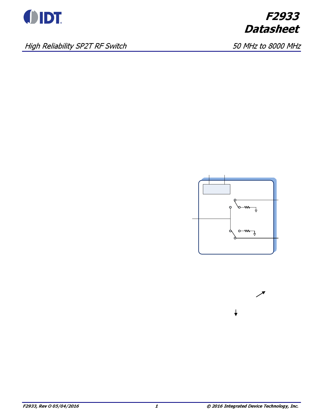
FUNCTIONAL BLOCK DIAGRAM
VDD VCTL
Control
Circuit
RFC
50Ω
50Ω
RF1
RF2
ORDERING INFORMATION
F2933NBGP8
Green
Tape &
Reel
F2933, Rev O 05/04/2016
1 © 2016 Integrated Device Technology, Inc.
1 page 
F2933
F2933 SPECIFICATION (CONT.)
Typical Application Circuit, VDD = 5.0 V, TC = +25 °C, FRF = 2000 MHz, Driven Port = RF1 or RF2, input power =
10 dBm, ZS = ZL = 50 ohms, PCB board trace and connector losses are de-embedded unless otherwise noted.
Parameter
Symbol
Condition
Min Typ Max Units
50 MHz
33.2
Input 1dB Compression3
ICP1dB
1 GHz
2 GHz
3 GHz
35.5
36.5 dBm
36.1
4 GHz
35.3
50 MHz
30.4
VDD = 5.0 V
2 GHz
3 GHz
32.3
32.6
Input 0.1dB Compression3 ICP0.1dB
4 GHz
50 MHz
32.2
30.1
dBm
VDD = 3.1 V
2 GHz
3 GHz
32.1
32.6
4 GHz
32.1
Input IP2
FRF1 = 2000 MHz, FRF2 = 1990 MHz
IIP2
RFIN = RF1 or RF2
PIN = +20 dBm / tone
111 dBm
FIP2 =FRF1 + FRF2
50 MHz
58
RF Input = RF1 or RF2 1 GHz
64
Input IP3
IIP3 PIN = +15 dBm/tone 2 GHz
∆ F = 1 MHz
2.5 GHz
64 dBm
63.4
4 GHz
63.6
Non-RF Driven Spurious4
At any RF port when externally
terminated into 50 Ω
-114
dBm
50% control to 90% RF
210
Switching Time5
TSW
50% control to 10% RF
50% control to RF settled to within
+/- 0.1 dB of I.L. value
115
225
ns
Maximum Switching Rate6 SWRATE
25 kHz
Maximum Video Feed-
through on RF Ports
VIDFT
5 MHz to 1000 MHz
Measured with 20 ns risetime,
0 to 3.3 V control pulse
12 mVpp
Note 1: Items in min/max columns in bold italics are Guaranteed by Test.
Note 2: Items in min/max columns that are not bold/italics are Guaranteed by Design Characterization.
Note 3: The input 1 dB compression point is a linearity figure of merit. Refer to the Recommended Operating
Conditions section for the specified maximum operating power levels.
Note 4: Spurious due to on-chip negative voltage generator. Typical generator fundamental frequency is 5.2 MHz.
Note 5: FRF = 1 GHz.
Note 6: Minimum time required between switching of states = 1/ (Maximum Switching Rate).
F2933, Rev O 05/04/2016
5 High Reliability SP2T RF Switch
5 Page 
LAND PATTERN DIMENSION
F2933
F2933, Rev O 05/04/2016
11 High Reliability SP2T RF Switch
11 Page | ||
| Páginas | Total 19 Páginas | |
| PDF Descargar | [ Datasheet F2933.PDF ] | |
Hoja de datos destacado
| Número de pieza | Descripción | Fabricantes |
| F2933 | High Reliability SP2T RF Switch | Integrated Device Technology |
| Número de pieza | Descripción | Fabricantes |
| SLA6805M | High Voltage 3 phase Motor Driver IC. |
Sanken |
| SDC1742 | 12- and 14-Bit Hybrid Synchro / Resolver-to-Digital Converters. |
Analog Devices |
|
DataSheet.es es una pagina web que funciona como un repositorio de manuales o hoja de datos de muchos de los productos más populares, |
| DataSheet.es | 2020 | Privacy Policy | Contacto | Buscar |