|
|
|
PDF TD7580 Data sheet ( Hoja de datos )
| Número de pieza | TD7580 | |
| Descripción | 4A 240KHZ 23V PWM Buck DC/DC Converter | |
| Fabricantes | Techcode | |
| Logotipo | ||
Hay una vista previa y un enlace de descarga de TD7580 (archivo pdf) en la parte inferior de esta página. Total 13 Páginas | ||
|
No Preview Available !
4A 240KHZ 23V PWM Buck DC/DC Converter
Datasheet
TD7580
General Description
Features
The TD7580 is a 240 KHz fixed frequency
monolithic step down switch mode regulator
with a built in internal Power MOSFET. It
achieves 4A continuous output current over a
wide input supply range with excellent load
and line regulation.
The device includes a voltage reference,
oscillation circuit, error amplifier, internal
PMOS and etc.
The PWM control circuit is able to adjust the
duty ratio linearly from 0 to 100%. An enable
function, an over current protection function
and a short circuit protection function are
built inside. An internal compensation block
is built in to minimize external component
count.
The TD7580 serves as ideal power supply
units for portable devices.
4A Constant Output Current
80mΩ RDSON Internal Power PMOSFET
Switch
Up to 95% Efficiency
Fixed 240KHz Frequency
Wide 3.6V to 23V Input Voltage Range
Output Adjustable from 1.222V to 21V
Built in Frequency Compensation
Built in Thermal Shutdown Function
Built in Current Limit Function
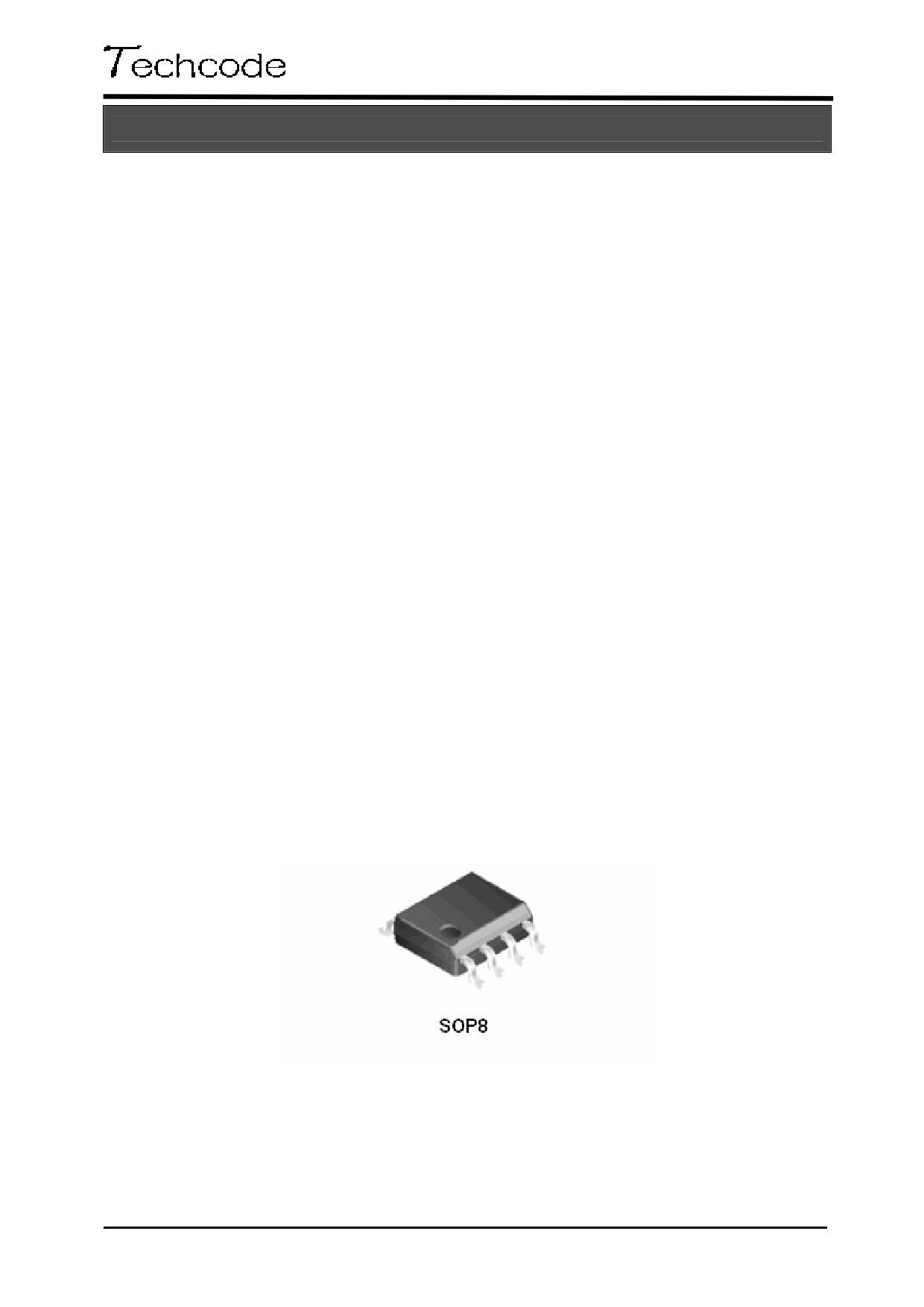
SOP-8 Package is Available
The minimum dropout up to 0.3V
Applications
Portable DVD
LCD Monitor / TV
Battery Charger
ADSL Modem
Telecom / Networking Equipment
Figure 1 Package Type of TD7580
September, 2006
Techcode Semiconductor Limited
1
1 page 
4A 240KHZ 23V PWM Buck DC/DC Converter
Typical Performance Characteristics
Datasheet
TD7580
Figure 4. Switching Frequency vs. Temperature
Figure 5. Vfb vs. Temperature
Figure 6. Icc vs. Temperature
Figure 7. Efficiency vs. Load (Vin=10V)
September, 2006
Techcode Semiconductor Limited
5
5 Page 
Datasheet
4A 240KHZ 23V PWM Buck DC/DC Converter
TD7580
This capacitor type can be ceramic, plastic, silver
mica, etc.(Because of the unstable characteristics
of ceramic capacitors made with Z5U material,
they are not recommended.)
Note:In PCB layout. Reserved an area for CFF.
Over Current Protection (OCP)
The cycle by cycle current limit threshold is set
between 5A and 5.6A. When the load current
reaches the current limit threshold, the cycle by
cycle current limit circuit turns off the high side
switch immediately to terminate the current duty
cycle. The inductor current stops rising. The cycle
by cycle current limit protection directly limits
inductor peak current. The average inductor
current is also limited due to the limitation on peak
inductor current. When the cycle by cycle current
limit circuit is triggered, the output voltage drops
as the duty cycle is decreasing.
Thermal Management and Layout
Consideration
In the TD7580 buck regulator circuit, high pulsing
current flows through two circuit loops. The first
loop starts from the input capacitors, to the VIN
pin, to the VOUT pins, to the filter inductor, to the
output capacitor and load, and then returns to the
input capacitor through ground.
Current flows in the first loop when the high side
switch is on. The second loop starts from the
inductor, to the output capacitors and load, to the
GND pin of the TD7580, and to the VOUT pins of
the TD7580. Current flows in the second loop
when the low side diode is on.
In PCB layout, minimizing the two loops area
reduces the noise of this circuit and improves
efficiency. A ground plane is recommended to
connect input capacitor, output capacitor, and
GND pin of the TD7580.
In the TD7580 buck regulator circuit, the two
major power dissipating components are the
TD7580 and output inductor. The total power
dissipation of converter circuit can be measured
by input power minus output power.
Ptotal _loss = V IN × IIN – V O × IO
The power dissipation of inductor can be
approximately calculated by output current and
DCR of inductor.
Pinductor _loss= IO 2 × Rinductor × 1.1
The junction to ambient temperature can be got
from power dissipation in the TD7580 and thermal
impedance from junction to ambient.
T (jun-amb) =(Ptotalloss–Pinductorloss)× ΘJA
The maximum junction temperature of TD7580 is
145°C, which limits the maximum load current
capability. Please see the thermal de-rating
curves for the maximum load current of the
TD7580 under different ambient temperatures.
The thermal performance of the TD7580 is trongly
affected by the PCB layout. Extra care should be
taken by users during the design process to nsure
that the IC will operate under the recommended
environmental conditions.
Several layout tips are listed below for the best
electric and thermal performance.
1. Do not use thermal relief connection to the VIN
and the GND pin. Pour a maximized copper area
to the GND pin and the VIN pin to help thermal
dissipation.
2. Input capacitor should be connected to the VIN
pin and the GND pin as close as possible.
3. Make the current trace from VOUT pins to L to
the GND as short as possible.
4. Pour copper plane on all unused board area
and connect it to stable DC nodes, like VIN, GND,
or VOUT.
5. Keep sensitive signal traces such as trace
connecting FB pin away from the VOUT pins.
September, 2006
Techcode Semiconductor Limited
11
11 Page | ||
| Páginas | Total 13 Páginas | |
| PDF Descargar | [ Datasheet TD7580.PDF ] | |
Hoja de datos destacado
| Número de pieza | Descripción | Fabricantes |
| TD7580 | 4A 240KHZ 23V PWM Buck DC/DC Converter | Techcode |
| Número de pieza | Descripción | Fabricantes |
| SLA6805M | High Voltage 3 phase Motor Driver IC. |
Sanken |
| SDC1742 | 12- and 14-Bit Hybrid Synchro / Resolver-to-Digital Converters. |
Analog Devices |
|
DataSheet.es es una pagina web que funciona como un repositorio de manuales o hoja de datos de muchos de los productos más populares, |
| DataSheet.es | 2020 | Privacy Policy | Contacto | Buscar |