|
|
|
PDF 74HC14 Data sheet ( Hoja de datos )
| Número de pieza | 74HC14 | |
| Descripción | Hex Schmitt-Trigger Inverter | |
| Fabricantes | ON Semiconductor | |
| Logotipo | ||
 1. inverting Schmitt trigger - NXP Hay una vista previa y un enlace de descarga de 74HC14 (archivo pdf) en la parte inferior de esta página. Total 9 Páginas | ||
|
No Preview Available !
74HC14
Hex Schmitt−Trigger
Inverter
High−Performance Silicon−Gate CMOS
The 74HC14 is identical in pinout to the LS14, LS04 and the HC04.
The device inputs are compatible with Standard CMOS outputs; with
pullup resistors, they are compatible with LSTTL outputs.
The HC14 is useful to “square up” slow input rise and fall times.
Due to hysteresis voltage of the Schmitt trigger, the HC14 finds
applications in noisy environments.
Features
• Output Drive Capability: 10 LSTTL Loads
• Outputs Directly Interface to CMOS, NMOS and TTL
• Operating Voltage Range: 2.0 to 6.0 V
• Low Input Current: 1.0 mA
• High Noise Immunity Characteristic of CMOS Devices
• In Compliance With the JEDEC Standard No. 7A Requirements
• ESD Performance: HBM > 2000 V; Machine Model > 200 V
• Chip Complexity: 60 FETs or 15 Equivalent Gates
• These are Pb−Free Devices
http://onsemi.com
MARKING
DIAGRAMS
14
1
14
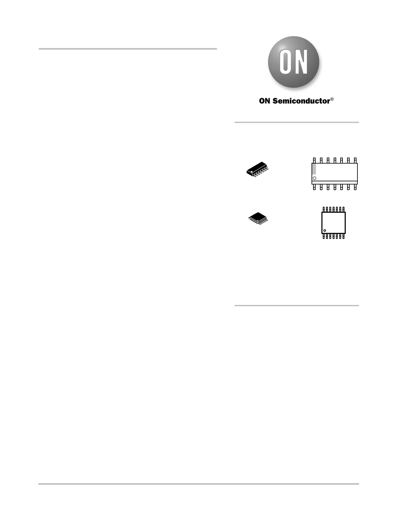
SOIC−14
D SUFFIX
CASE 751A
1
HC14G
AWLYWW
14
1
TSSOP−14
DT SUFFIX
CASE 948G
14
HC
14
ALYW G
1G
HC14 = Device Code
A = Assembly Location
L, WL = Wafer Lot
Y = Year
W, WW = Work Week
G or G = Pb−Free Package
(Note: Microdot may be in either location)
ORDERING INFORMATION
See detailed ordering and shipping information in the package
dimensions section on page 2 of this data sheet.
© Semiconductor Components Industries, LLC, 2007
March, 2007 − Rev. 1
1
Publication Order Number:
74HC14/D
1 page 
74HC14
AC CHARACTERISTICS (CL = 50pF, Input tr = tf = 6ns)
Symbol
Parameter
VCC Guaranteed Limit
(V) −55 to 25°C ≤85°C
≤125°C
Unit
tPLH,
tPHL
Maximum Propagation Delay, Input A or B to Output Y
(Figures 1 and 2)
2.0 75
3.0 30
4.5 15
6.0 13
95 110 ns
40 55
19 22
16 19
tTLH,
tTHL
Maximum Output Transition Time, Any Output
(Figures 1 and 2)
2.0 75
3.0 27
4.5 15
6.0 13
95 110 ns
32 36
19 22
16 19
Cin Maximum Input Capacitance
10 10 10 pF
NOTE: For propagation delays with loads other than 50 pF, and information on typical parametric values, see Chapter 2 of the ON
Semiconductor High−Speed CMOS Data Book (DL129/D).
Typical @ 25°C, VCC = 5.0 V
CPD Power Dissipation Capacitance (Per Inverter)*
22 pF
* Used to determine the no−load dynamic power consumption: PD = CPD VCC2f + ICC VCC. For load considerations, see Chapter 2 of the
ON Semiconductor High−Speed CMOS Data Book (DL129/D).
tf tr
INPUT A
90%
50%
10%
OUTPUT Y
tPLH
90%
50%
10%
tTLH
tPHL
Figure 1. Switching Waveforms
VCC
GND
tTHL
DEVICE
UNDER
TEST
TEST
POINT
OUTPUT
CL*
*Includes all probe and jig capacitance
Figure 2. Test Circuit
http://onsemi.com
5
5 Page | ||
| Páginas | Total 9 Páginas | |
| PDF Descargar | [ Datasheet 74HC14.PDF ] | |
Hoja de datos destacado
| Número de pieza | Descripción | Fabricantes |
| 74HC10 | Triple 3-input NAND gate | Philips |
| 74HC107 | Dual JK flip-flop with reset negative-edge trigger | Philips |
| 74HC109 | Dual JK flip-flop with set and reset positive-edge trigger | Philips |
| 74HC11 | Triple 3-input AND gate | Philips |
| Número de pieza | Descripción | Fabricantes |
| SLA6805M | High Voltage 3 phase Motor Driver IC. |
Sanken |
| SDC1742 | 12- and 14-Bit Hybrid Synchro / Resolver-to-Digital Converters. |
Analog Devices |
|
DataSheet.es es una pagina web que funciona como un repositorio de manuales o hoja de datos de muchos de los productos más populares, |
| DataSheet.es | 2020 | Privacy Policy | Contacto | Buscar |