|
|
PDF QN8007B Data sheet ( Hoja de datos )
| Número de pieza | QN8007B | |
| Descripción | High Performance Digital FM Transmitter | |
| Fabricantes | Quintic | |
| Logotipo |  |
|
Hay una vista previa y un enlace de descarga de QN8007B (archivo pdf) en la parte inferior de esta página. Total 30 Páginas | ||
|
No Preview Available !
QN8007B/8007LB
High Performance Digital FM Transmitter for Portable Devices
____________________________ General Description ________________________
The QN8007 is a high performance, low power, full-featured single-chip stereo FM transmitter designed for portable
audio/video players, automotive accessories, cell phones, and GPS personal navigation devices. It integrates transmitting
functions, clear channel scan, and antenna tuning to ease matching in real applications. Advanced digital architecture
enables variable input gain programming; selectable pre-emphasis, precision low-spur MPX stereo encoding and pilot tone
generation, low-noise PLL-based modulation, and an on-chip power amplifier with variable output level and RF band-pass
filtering to ensure optimum transmit spectrum purity.
With its small footprint, minimal external component count and multiple clock frequency support, the QN8007 is easy to
integrate into a variety of small form-factor low power portable applications. An integrated voltage regulator enables direct
connection to a battery and provides high PSRR for superior noise suppression. A low-power Standby mode extends battery
life. ESD protection is on all pins. The QN8007 is fabricated in highly reliable CMOS technology.
_____________________________ Key Features _____________________________
Worldwide FM Band Transmit
• 76 MHz to 108 MHz full band tuning in
50/100/200 kHz step sizes
• 50/75s pre-emphasis
High Performance FM Transmitter (FMT)
• 66dB Stereo SNR, 0.03% THD
• Maximum 121dBµV RF output level with 42dB
adjustable range
• Integrated Clear Channel Scan
RDS/RBDS Transmit
• Supports US and European data service,
including TMC (Traffic Messaging Channel)
(not available in QN8007L)
Flexible Audio Interfaces
• Digital audio interface supports I2S and a variety
of PCM data formats with 4 different data rates
• Programmable analog audio input/output
• Integrated audio AGC and soft clipping
Very Low Power Consumption
• 9.2 mA
• Integrated voltage regulator, direct connect to battery
• Power saving idle and standby modes
• Low shutdown leakage current
Ease of Integration
• Small footprint, 4 x 4 x 0.85mm QFN24
• Only 2 external passive components required
• Adaptive antenna tuning
• Low cellular and GPS band spurs
• High Immunity to TDMA (GSM/GPRS) burst noise
• Multiple crystal frequencies supported
• 2-wire and 3-wire control interfaces
Robust Operation
• -250C to +850C operation
• ESD protection on all input and output pads
_____________________________ Typical Applications __________________________
Cell Phones / PDAs / Smart Phones
Portable Audio & Media Players
GPS Personal Navigation Devices
Automotive and Accessories
Rev 2.09 (11/09)
Confidential A
Copyright ©2009 by Quintic Corporation
Confidential Information contained herein is covered under Non-Disclosure Agreement (NDA).
Page 1
1 page 
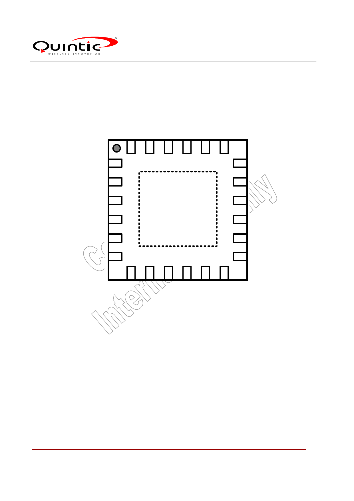
2 PIN ASSIGNMENTS
QN8007B/8007LB
(Top View)
N/C 1
N/C 2
AUGND 3
ALI 4
ARI 5
AGND 6
Exposed Pad
Pin 25
(AGND)
- far side -
18 XTAL2
17 XTAL1
16 XCLK
15 WS
14 INT
13 MCK
Figure 2: QN8007B Device Pin Out
Rev 2.09 (11/09)
Confidential A
Copyright ©2009 by Quintic Corporation
Page 5
Confidential Information contained herein is covered under Non-Disclosure Agreement (NDA).
5 Page 
QN8007B/8007LB
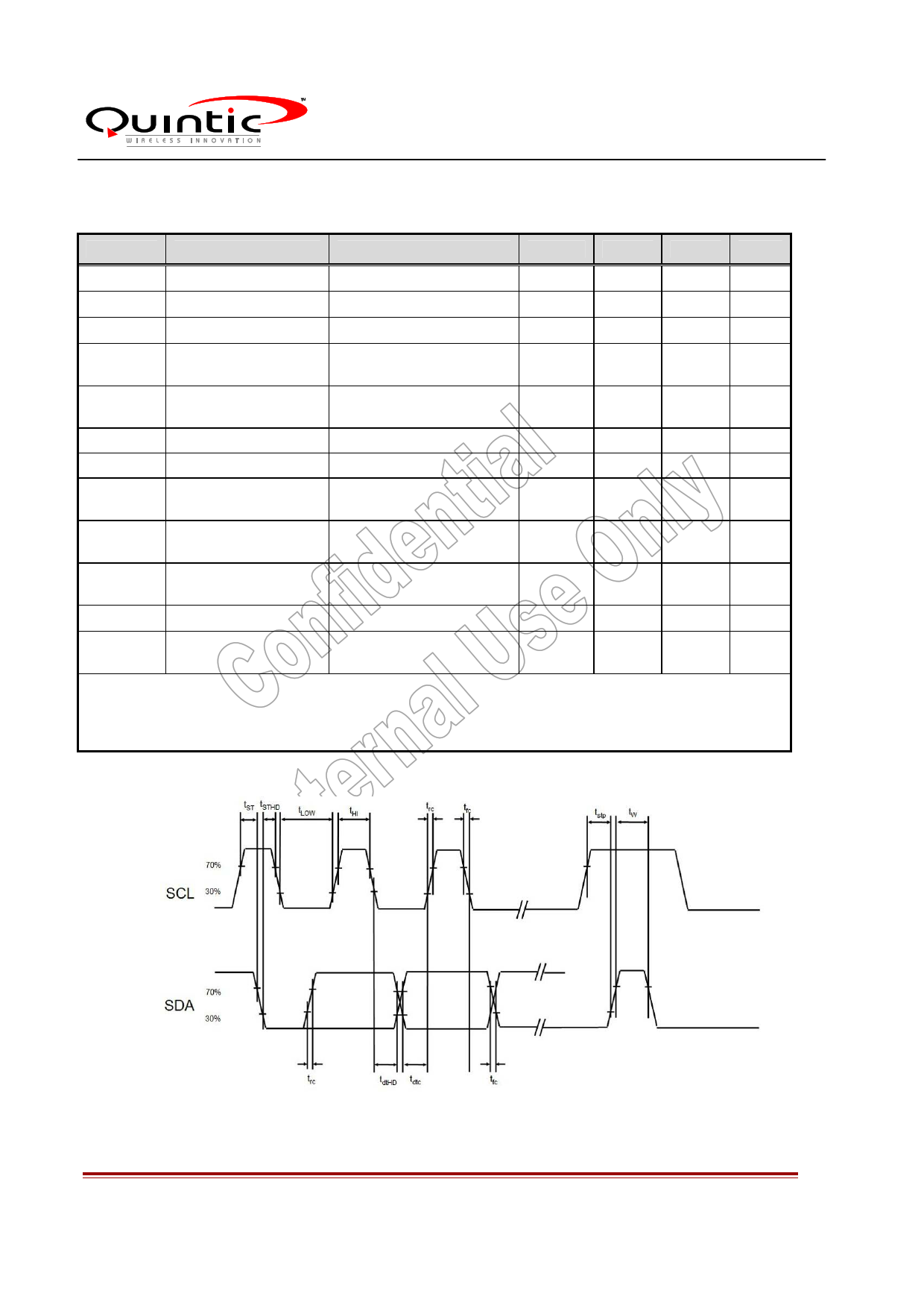
Table 8: 2-Wire Interface Timing Characteristics
(Vcc = 2.7 ~ 5.0 V, TA = -25 ~ 85 oC, unless otherwise noticed. Typical values are at Vcc = 3.3V and TA = 25oC).
SYMBOL
PARAMETER
CONDITIONS
fSCL 2-wire clock frequency
tLOW Clock Low time
tHI Clock High time
tST
SCL input to SDA
falling edge start 1,3
tSTHD
SDA falling edge to
SCL falling edge start3
trc SCL rising edge3
Level from 30% to 70%
tfc SCL falling edge3
Level from 70% to 30%
tdtHD
SCL falling edge to
next SDA rising edge3
tdtc
SDA rising edge to
next SCL rising edge3
tstp
SCL rising edge to
SDA rising edge 2,3
tw Duration before restart3
Cb
SCL, SDA capacitive
loading3
Notes:
1. Start signaling of 2-wire interface.
2. Stop signaling of 2-wire interface.
3. Guaranteed by design.
MIN
1.3
0.8
0.6
0.6
20
0.6
1.3
TYP
10
MAX
400
UNIT
kHz
s
s
s
s
300 ns
300 ns
ns
900 ns
s
s
pF
Figure 3: 2-wire Serial Control Interface Timing Diagram
Rev 2.09 (11/09)
Confidential A
Copyright ©2009 by Quintic Corporation
Page 11
Confidential Information contained herein is covered under Non-Disclosure Agreement (NDA).
11 Page | ||
| Páginas | Total 30 Páginas | |
| PDF Descargar | [ Datasheet QN8007B.PDF ] | |
Hoja de datos destacado
| Número de pieza | Descripción | Fabricantes |
| QN8007B | High Performance Digital FM Transmitter | Quintic |
| QN8007LB | High Performance Digital FM Transmitter | Quintic |
| Número de pieza | Descripción | Fabricantes |
| SLA6805M | High Voltage 3 phase Motor Driver IC. |
Sanken |
| SDC1742 | 12- and 14-Bit Hybrid Synchro / Resolver-to-Digital Converters. |
Analog Devices |
|
DataSheet.es es una pagina web que funciona como un repositorio de manuales o hoja de datos de muchos de los productos más populares, |
| DataSheet.es | 2020 | Privacy Policy | Contacto | Buscar |
