|
|
|
PDF CLC5633IMX Data sheet ( Hoja de datos )
| Número de pieza | CLC5633IMX | |
| Descripción | Triple/ High Output/ Programmable Gain Buffer | |
| Fabricantes | National Semiconductor | |
| Logotipo | ||
Hay una vista previa y un enlace de descarga de CLC5633IMX (archivo pdf) en la parte inferior de esta página. Total 12 Páginas | ||
|
No Preview Available !
N
CLC5633
Triple, High Output, Programmable Gain Buffer
June 1999
General Description
The CLC5633 is a triple, low-cost, high-speed (130MHz) buffer
which features user-programmable gains of +2, +1, and -1V/V.
The CLC5633 also has a new output stage that delivers high
output drive current (130mA), but consumes minimal quiescent
supply current (3.0mA/ch) from a single 5V supply. Its current
feedback architecture, fabricated in an advanced complementary
bipolar process, maintains consistent performance over a wide
range of gains and signal levels, and has a linear-phase response
up to one half of the -3dB frequency.
The CLC5633 offers 0.1dB gain flatness to 20MHz and differen-
tial gain and phase errors of 0.03% and 0.06°. These features are
ideal for professional and consumer video applications.
The CLC5633 offers superior dynamic performance with a
130MHz small-signal bandwidth, 410V/µs slew rate and 5.0ns
rise/fall times (2Vstep). The combination of low quiescent power,
high output current drive, and high-speed performance make
the CLC5633 well suited for many battery-powered personal
communication/computing systems.
The ability to drive low-impedance, highly capacitive loads,
with minimum distortion makes the CLC5633 ideal for cable
applications. The CLC5633 will drive a 100Ω load with only
-73/-92dBc second/third harmonic distortion (Av = +2, Vout =
2Vpp, f = 1MHz). With a 25Ω load, and the same conditions, it
produces only -75/-75dBc second/third harmonic distortion. It is
also optimized for driving high currents into single-ended
transformers and coils.
When driving the input of high-resolution A/D converters, the
CLC5633 provides excellent -92/-96dBc second/third harmonic
distortion (Av = +2, Vout = 2Vpp, f = 1MHz, RL = 1kΩ) and fast
settling time.
Features
s 130mA output current
s 0.03%, 0.06° differential gain, phase
s 3.0mA/ch supply current
s 130MHz bandwidth (Av = +2)
s -92/-96dBc HD2/HD3 (1MHz)
s 20ns settling to 0.05%
s 410V/µs slew rate
s Stable for capacitive loads up to 1000pf
s Single 5V to ±5V supplies
Applications
s Video line driver
s Coaxial cable driver
s Twisted pair driver
s Transformer/coil driver
s High capacitive load driver
s Portable/battery-powered applications
s A/D driver
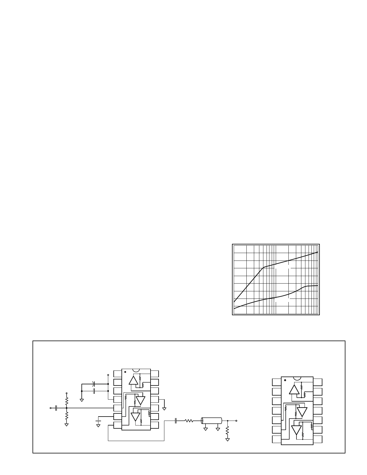
Maximum Output Voltage vs. RL
10
9
8
7 VCC = ±5V
6
5
4
3 Vs = +5V
2
1
10 100
RL (Ω)
1000
Typical Application
Single Supply Cable Driver
+5V 1
6.8µF
+2
+5V
Vin 0.1µF 5kΩ
0.1µF
3
4
5
5kΩ
0.1µF
6
7
14
1kΩ
1kΩ 13
12
1kΩ - +
1kΩ
11
10
+ - 1kΩ
1kΩ
9
8
CLC5633
Note: Channel 2 and 3 not shown.
10m of 75Ω
75Ω Coaxial Cable
Vo
0.1µF
75Ω
Pinout
DIP & SOIC
NC 1
NC 2
NC 3
+Vs 4
+IN1 5
-IN1 6
OUT1 7
14
1kΩ
1kΩ 13
12
1kΩ - +
1kΩ
11
10
+ - 1kΩ
1kΩ
9
8
OUT2
-IN2
+IN2
-Vs
+IN3
-IN3
OUT3
© 1999 National Semiconductor Corporation
Printed in the U.S.A.
http://www.national.com
1 page 
±5V Typical Performance (Av = +2, RL = 100Ω, VCC = ± 5V, unless specified)
Frequency Response
Vo = 1.0Vpp
Gain
Av = -1
Av = +1
Phase
Av = +2
1M 10M 100M
Frequency (Hz)
Frequency Response vs. Vo (Av = 2)
0
-45
-90
-135
-180
-225
Vo = 0.1Vpp
Frequency Response vs. RL
Vo = 1.0Vpp
Gain
RL = 1kΩ
Phase
1M
RL = 100Ω
RL = 25Ω
10M
Frequency (Hz)
100M
0
-90
-180
-270
-360
-450
Frequency Response vs. Vo (Av = 1)
Vo = 1Vpp
Vo = 0.1Vpp
Vo = 5Vpp
Vo = 2Vpp
Vo = 5Vpp
Vo = 1Vpp
Vo = 2Vpp
Gain Flatness & Linear Phase
Gain
VO = 1Vpp
0
-0.1
-0.2
Phase
-0.3
-0.4
-0.5
0 5 10 15 20 25 30
Frequency (MHz)
Frequency Response vs. Vo (Av = -1)
Vo = 1Vpp
Vo = 5Vpp
Vo = 0.1Vpp
Vo = 2Vpp
1M 10M 100M
Frequency (Hz)
Large & Small Signal Pulse Response
Large Signal
Small Signal
Time (10ns/div)
2nd & 3rd Harmonic Distortion, RL = 25Ω
-45
2nd, 10MHz
-50
-55 3rd, 10MHz
-60
-65
-70
-75 2nd, 1MHz
-80
-85
0
3rd, 1MHz
0.5 1 1.5 2
Output Amplitude (Vpp)
2.5
Short Term Settling Time
0.2
0.15
0.1
0.05
0
-0.05
-0.1
-0.15
-0.2
1
10 100
Time (ns)
Vo = 2V step
1000 10000
1M 10M 100M
Frequency (Hz)
Differential Gain & Phase
0.02
f = 3.58MHz
0
Phase Neg Sync
-0.02
-0.04
Gain Neg Sync
-0.02
-0.04
-0.06
-0.08
-0.06 -0.1
-0.08
-0.1
Gain Pos Sync
Phase Pos Sync
-0.12
-0.14
-0.12
1
23
Number of 150 Ω Loads
-0.16
4
2nd & 3rd Harmonic Distortion, RL = 100Ω
-60
3rd, 10MHz
-65
2nd, 10MHz
-70
-75
2nd, 1MHz
-80
-85
3rd, 1MHz
-90
-95
0
0.5 1 1.5 2
Output Amplitude (Vpp)
2.5
Long Term Settling Time
0.2
0.15
0.1
0.05
0
Vo = 2V step
-0.05
-0.1
-0.15
-0.2
1µ
10µ 100µ
1m
Time (s)
10m
5
1M 10M 100M
Frequency (Hz)
2nd & 3rd Harmonic Distortion
-60
Vo = 2Vpp
2nd
-70 RL = 100Ω
2nd
-80 RL = 1kΩ
3rd
RL = 100Ω
-90
3rd
RL = 1kΩ
-100
1
Frequency (MHz)
10
2nd & 3rd Harmonic Distortion, RL = 1kΩ
-60
-70 2nd, 10MHz
3rd, 10MHz
-80
-90 2nd, 1MHz
-100 3rd, 1MHz
-110
0
1 2 34
Output Amplitude (Vpp)
IBN & VOS vs. Temperature
7.5
5
2.5
7.0 1.5
6.5 0.5
6.0
5.5
5.0
-60
-0.5
VOS
-1.5
IBN
-20 20 60
Temperature (°C)
-2.5
100
http://www.national.com
5 Page 
This page intentionally left blank.
11 http://www.national.com
11 Page | ||
| Páginas | Total 12 Páginas | |
| PDF Descargar | [ Datasheet CLC5633IMX.PDF ] | |
Hoja de datos destacado
| Número de pieza | Descripción | Fabricantes |
| CLC5633IM | Triple/ High Output/ Programmable Gain Buffer | National Semiconductor |
| CLC5633IMX | Triple/ High Output/ Programmable Gain Buffer | National Semiconductor |
| Número de pieza | Descripción | Fabricantes |
| SLA6805M | High Voltage 3 phase Motor Driver IC. |
Sanken |
| SDC1742 | 12- and 14-Bit Hybrid Synchro / Resolver-to-Digital Converters. |
Analog Devices |
|
DataSheet.es es una pagina web que funciona como un repositorio de manuales o hoja de datos de muchos de los productos más populares, |
| DataSheet.es | 2020 | Privacy Policy | Contacto | Buscar |