|
|
|
PDF CLC5622IM Data sheet ( Hoja de datos )
| Número de pieza | CLC5622IM | |
| Descripción | Dual/ High Output/ Video Amplifier | |
| Fabricantes | National Semiconductor | |
| Logotipo | ||
Hay una vista previa y un enlace de descarga de CLC5622IM (archivo pdf) en la parte inferior de esta página. Total 12 Páginas | ||
|
No Preview Available !
N
CLC5622
Dual, High Output, Video Amplifier
June 1999
General Description
The National CLC5622 has a new output stage that delivers high
output drive current (130mA), but consumes minimal
quiescent supply current (3.0mA/ch) from a single 5V supply. Its
current feedback architecture, fabricated in an advanced comple-
mentary bipolar process, maintains consistent performance over
a wide range of gains and signal levels, and has a linear-phase
response up to one half of the -3dB frequency.
The CLC5622 offers 0.1dB gain flatness to 30MHz and differen-
tial gain and phase errors of 0.05% and 0.03°. These features are
ideal for professional and consumer video applications.
The CLC5622 offers superior dynamic performance with a
160MHz small-signal bandwidth, 370V/µs slew rate and 4.4ns
rise/fall times (2Vstep). The combination of low quiescent power,
high output current drive, and high-speed performance make
the CLC5622 well suited for many battery-powered personal
communication/computing systems.
The ability to drive low-impedance, highly capacitive loads,
makes the CLC5622 ideal for single ended cable applications.
It also drives low impedance loads with minimum distortion.
The CLC5622 will drive a 100Ω load with only -95/-95dBc
second/third harmonic distortion (Av = +2, Vout = 2Vpp, f = 1MHz).
With a 25Ω load, and the same conditions, it produces only -72/
-77dBc second/third harmonic distortion.
The CLC5622 can also be used for driving differential-input step-
up transformers for applications such as Asynchronous Digital
Subscriber Lines (ADSL) or High-Bit-Rate Digital Subscriber
Lines (HDSL).
When driving the input of high-resolution A/D converters, the
CLC5622 provides excellent -90/-97dBc second/third harmonic
distortion (Av = +2, Vout = 2Vpp, f = 1MHz, RL = 1kΩ) and fast
settling time.
Features
s 130mA output current
s 0.05%, 0.03° differential gain, phase
s 3.0mA/ch supply current
s 160MHz bandwidth (Av = +2)
s -90/-97dBc HD2/HD3 (1MHz)
s 18ns settling to 0.05%
s 370V/µs slew rate
s Stable for capacitive loads up to 1000pf
s Single 5V or ±5V supplies
Applications
s Video line driver
s ADSL/HDSL driver
s Coaxial cable driver
s UTP differential line driver
s Transformer/coil driver
s High capacitive load driver
s Portable/battery-powered applications
s Differential A/D driver
Maximum Output Voltage vs. RL
10
9
8
7 VCC = ±5V
6
5
4
3 Vs = +5V
2
1
10 100
RL (Ω)
1000
Typical Application
Differential Line Driver with Load Impedance Conversion
Rg2
Vin
Rt1
Vd/2
+
1/2
CLC5622
-
Rf1
Rg1 Rt2
Rf2
-
1/2
CLC5622
+
-Vd/2
Rm/2
Req
Rm/2
1:n
Zo
UTP
Io
RL
+
Vo
-
Vo1
Vinv1
Vnon-inv1
-VCC
Pinout
DIP & SOIC
+VCC
Vo2
Vinv2
Vnon-inv2
© 1999 National Semiconductor Corporation
Printed in the U.S.A.
http://www.national.com
1 page 
±5V Typical Performance (Av = +2, Rf = 750Ω, RL = 100Ω, VCC = ±5V, unless specified)
Frequency Response
Inverting Frequency Response
Frequency Response vs. RL
Vo = 1.0Vpp
Gain
Phase
Av = +1
Rf = 1.2kΩ
Av = +2
Rf = 649Ω
Av = +5
Rf = 402Ω
Av = +10
Rf = 200Ω
1M 10M 100M
Frequency (Hz)
0
-45
-90
-135
-180
-225
Frequency Response vs. Vo
Vo = 0.1Vpp
Vo = 1Vpp
Vo = 5Vpp
Vo = 2Vpp
Vo = 1.0Vpp
Gain
Av = -2
Rf = 649Ω
Phase
Av = -1
Rf = 1.2kΩ
Av = -5
Rf = 500Ω
Av = -10
Rf = 500Ω
1M 10M 100M
Frequency (Hz)
180
135
90
45
0
-45
Gain Flatness & Linear Phase
0.3
Gain
Phase
0.2
0.1
0
Vo = 1.0Vpp
RL = 1kΩ
Gain
Phase
RL = 100Ω
RL = 25Ω
1M 10M 100M
Frequency (Hz)
0
-90
-180
-270
-360
-450
Small Signal Pulse Response
Av = +2
Av = -2
1M 10M 100M
Frequency (Hz)
Large Signal Pulse Response
Av = +2
Av = -2
Time (10ns/div)
2nd & 3rd Harmonic Distortion, RL = 25Ω
-40
-50
3rd, 10MHz
-60
2nd, 10MHz
-70
-80
-90
0
2nd, 1MHz
3rd, 1MHz
1 2 34
Output Amplitude (Vpp)
5
Short Term Settling Time
0.2
0.15
0.1
0.05
0
-0.05
-0.1
-0.15
-0.2
1
10 100
Time (ns)
1000
10000
-0.1
0 5 10 15 20 25 30
Frequency (MHz)
Differential Gain & Phase
0.1
0.01
0
Gain Pos Sync
-0.1
0
-0.01
-0.2 -0.02
Phase Neg Sync
-0.3 -0.03
Gain Neg Sync
-0.4 -0.04
Phase Pos Sync
-0.5 -0.05
-0.6
1
23
Number of 150 Ω Loads
-0.06
4
2nd & 3rd Harmonic Distortion, RL = 100Ω
-60
3rd, 10MHz
-70
2nd, 10MHz
-80
-90 2nd, 1MHz
-100
0
3rd, 1MHz
0.5 1 1.5 2
Output Amplitude (Vpp)
2.5
Long Term Settling Time
0.2
0.15
0.1
0.05
0
-0.05
-0.1
-0.15
-0.2
1µ
10µ 100µ
1m
Time (s)
10m 100m
5
Time (10ns/div)
2nd & 3rd Harmonic Distortion
-50
Vo = 2Vpp
3rd
-60 RL = 100Ω
-70
2nd
RL = 1kΩ
-80
2nd
-90
RL = 100Ω
3rd
RL = 1kΩ
-100
1M
Frequency (Hz)
10M
2nd & 3rd Harmonic Distortion, RL = 1kΩ
-50
-60 3rd, 10MHz
-70 2nd, 10MHz
-80 2nd, 1MHz
-90
3rd, 1MHz
-100
-110
-120
0
1 2 34
Output Amplitude (Vpp)
5
IBI, IBN, VOS vs. Temperature
4 10
3 IBI
6
2
1
0
-100
2
VOS
IBN
-50 0 50 100
Temperature (°C)
-2
-6
150
http://www.national.com
5 Page 
where Zo(5622)(jω) is the output impedance of the
CLC5622 and |Zo(5622)(jω)| << Rm.
The load voltage and current will fall in the ranges:
Vo ≤ n ⋅ Vmax
Io
≤ Imax
n
The CLC5622’s high output drive current and low
distortion make it a good choice for this application.
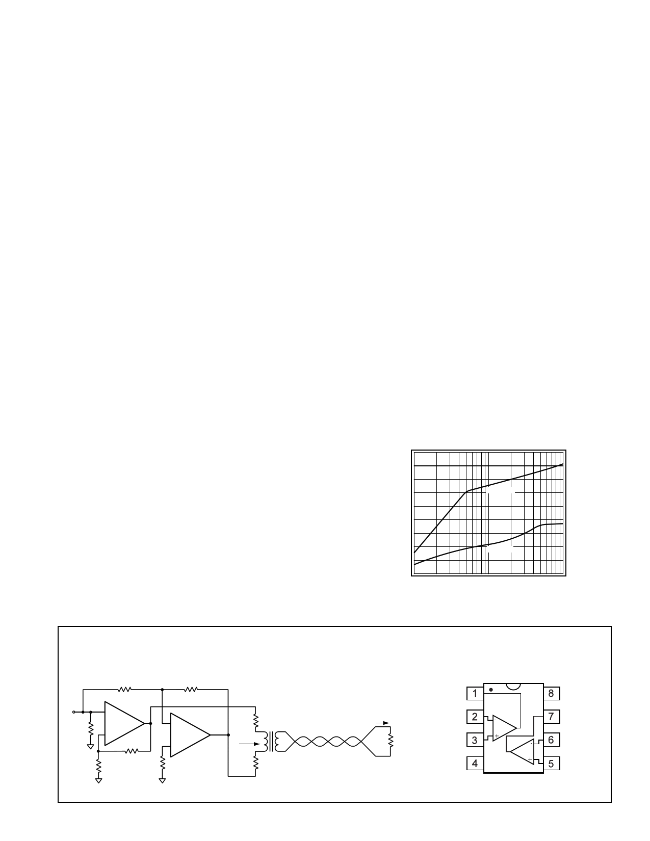
Full Duplex Cable Driver
The circuit shown in Figure 16 below, operates as a full
duplex cable driver which allows simultaneous transmis-
sion and reception of signals on one transmission line.
The circuit on either side of the transmission line uses are
CLC5622 as a cable driver, and the second CLC5622 as
a receiver. VoA is an attenuated version of VinA, while VoB
is an attenuated version of VinB.
VinA
Rt1
VoB
+
1/2
CLC5622
-
Rm1
Rf1 Rg2
Rf2
-
1/2
CLC5622
+
Rt2
Z0
Rm1
+
1/2
CLC5622
-
Rg2 Rf1
Rf2
-
1/2
Rt2 CLC5622
+
VinB
Rt1
VoA
Figure 16: Full Duplex Cable Driver
Rm1 is used to match the transmission line. Rf2 and Rg2
set the DC gain of the CLC5622, which is used in a
difference mode. Rt2 provides good CMRR and DC
offset. The transmitting CLC5622’s are shown in a unity
gain configuration because they consume the least
power of any gain, for a given load. For proper operation
we need Rf2 = Rg2.
The receiver output voltages are:
VoutA(B)
≈
VinA(B) ⋅ A
+
VinB(A)
2
⋅ 1−
Rf2
Rg2
+
Zo(5622)(jω)
Rm1
where A is the attenuation of the cable, Zo(5622)(jω) is the
output impedance of the CLC5622 (see the Closed-Loop
Output Resistance plot), and |Zo(5622)(jω)| << Rm1.
We selected the component values as follows:
s Rf1 = 1.2kΩ, the recommended value for
CLC5622 at unity gain
s Rm1 = Zo = 50Ω, the characteristic impedance
of the transmission line
s Rf2 = Rg2 = 750Ω ≥ Rm1, the recommended
value for the CLC5622 at Av = 2
s
Rt2
=
(Rf2
|| Rg2 ) –
Rm1
2
=
25Ω
These values give excellent isolation from the other input:
VoA(B) ≈ −38dB, f = 5.0MHz
VinB(A)
The CLC5622 provides large output current drive, while
consuming little supply current, at the nominal bias point.
It also produces low distortion with large signal swings
and heavy loads. These features make the CLC5622 an
excellent choice for driving transmission lines.
11 http://www.national.com
11 Page | ||
| Páginas | Total 12 Páginas | |
| PDF Descargar | [ Datasheet CLC5622IM.PDF ] | |
Hoja de datos destacado
| Número de pieza | Descripción | Fabricantes |
| CLC5622IM | Dual/ High Output/ Video Amplifier | National Semiconductor |
| CLC5622IMX | Dual/ High Output/ Video Amplifier | National Semiconductor |
| CLC5622IN | Dual/ High Output/ Video Amplifier | National Semiconductor |
| Número de pieza | Descripción | Fabricantes |
| SLA6805M | High Voltage 3 phase Motor Driver IC. |
Sanken |
| SDC1742 | 12- and 14-Bit Hybrid Synchro / Resolver-to-Digital Converters. |
Analog Devices |
|
DataSheet.es es una pagina web que funciona como un repositorio de manuales o hoja de datos de muchos de los productos más populares, |
| DataSheet.es | 2020 | Privacy Policy | Contacto | Buscar |