|
|
|
PDF CLC425AJE Data sheet ( Hoja de datos )
| Número de pieza | CLC425AJE | |
| Descripción | Ultra Low Noise Wideband Op Amp | |
| Fabricantes | National Semiconductor | |
| Logotipo | ||
Hay una vista previa y un enlace de descarga de CLC425AJE (archivo pdf) en la parte inferior de esta página. Total 9 Páginas | ||
|
No Preview Available !
N
CLC425
Ultra Low Noise Wideband Op Amp
June 1999
General Description
The CLC425 combines a wide bandwidth (1.9GHz GBW) with very
low input noise (1.05nV/√Hz, 1.6pA/√Hz) and low dc errors (100µV
VOS, 2µV/°C drift) to provide a very precise, wide dynamic-range
op amp offering closed-loop gains of ≥10.
Singularly suited for very wideband high-gain operation, the CLC425
employs a traditional voltage-feedback topology providing all the
benefits of balanced inputs, such as low offsets and drifts, as well
as a 96dB open-loop gain, a 100dB CMRR and a 95dB PSRR.
The CLC425 also offers great flexibility with its externally adjustable
supply current, allowing designers to easily choose the optimum
set of power, bandwidth, noise and distortion performance.
Operating from ±5V power supplies, the CLC425 defaults to a
15mA quiescent current, or by adding one external resistor, the
supply current can be adjusted to less than 5mA.
The CLC425's combination of ultra-low noise, wide gain-band-
width, high slew rate and low dc errors will enable applications in
areas such as medical diagnostic ultrasound, magnetic tape & disk
storage, communications and opto-electronics to achieve maximum
high-frequency signal-to-noise ratios.
The CLC425 is available in the following versions:
CLC425AJP
CLC425AJE
CLC425A8B
-40°C to +85°C
-40°C to +85°C
-55°C to +125°C
CLC425ALC -40°C to +85°C
CLC425AMC -55°C to +125°C
CLC425AJM5 -40°C to +85°C
DESC SMD number : 5962-93259.
8-pin PDIP
8-pin SOIC
8-pin CERDIP,
MIL-STD-883, Level B
dice
dice, MIL-STD-883, Level B
5-pin SOT
Features
s 1.9GHz gain-bandwidth product
s 1.05nV/√Hz input voltage noise
s 0.8pA/√Hz @ Icc < 5mA
s 100µV input offset voltage, 2µV/°C drift
s 350V/µs slew rate
s 15mA to 5mA adjustable supply current
s Gain range ±10 to ±1,000V/V
s Evaluation boards & simulation
macromodel
s 0.9dB NF @ Rs = 700Ω
Applications
s Instrumentation sense amplifiers
s Ultrasound pre-amps
s Magnetic tape & disk pre-amps
s Photo-diode transimpedance amplifiers
s Wide band active filters
s Low noise figure RF amplifiers
s Professional audio systems
s Low-noise loop filters for PLLs
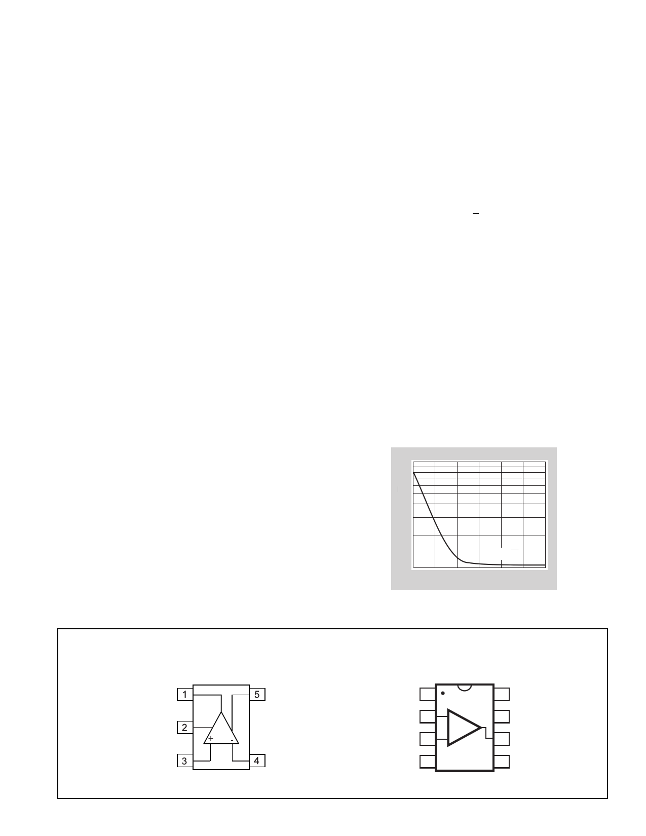
Equivalent Input Voltage Noise
10
1.05nV/√Hz
1
100 1k 10k 100k 1M 10M 100M
Frequency (Hz)
Vo
VEE
Vnon-inv
Pinout
SOT23-5
VCC
Vinv
© 1999 National Semiconductor Corporation
Printed in the U.S.A.
Pinout
DIP & SOIC
NC 1
Vinv 2
Vnon-inv 3
-Vcc 4
-
+
8 Rp (optional)
7 +Vcc
6 Vout
5 NC
http://www.national.com
1 page 
Vin
Rs
Vs RT
Rseq = Rs || RT
+Vcc
6.8µF
37
0.1µF
CLC425
2
6.8µF
4
6
Vout
-Vcc 0.1µF
Rf
Rg
Av
=1
+
Rf
Rg
Figure 1: Non-inverting Amplifier Configuration
Introduction
The CLC425 is a very wide gain-bandwidth, ultra-low
noise voltage feedback operational amplifier which en-
ables application areas such as medical diagnostic ultra-
sound, magnetic tape & disk storage and fiber-optics to
achieve maximum high-frequency signal-to-noise ratios.
The set of characteristic plots located in the "Typical
Performance" section illustrates many of the perfor-
mance trade-offs. The following discussion will enable
the proper selection of external components in order to
achieve optimum device performance.
Total Input Noise vs. Source Resistance
In order to determine maximum signal-to-noise ratios
from the CLC425, an understanding of the interaction
between the amplifier's intrinsic noise sources and the
noise arising from its external resistors is necessary.
Figure 3 describes the noise model for the non-inverting
amplifier configuration showing all noise sources. In
addition to the intrinsic input voltage noise (en) and
current noise (in=in+=in-) sources, there also exists ther-
mal voltage noise (et = 4kTR ) associated with each of
the external resistors. Equation 1 provides the general
form for total equivalent input voltage noise density (eni).
Equation 2 is a simplification of Equation 1 that assumes
Rseq
√4kTRseq
en
in+ CLC425
Rg Rf √4kTRf
in-
√4kTRg
Bias Current Cancellation
In order to cancel the bias current errors of the non-
inverting configuration, the parallel combination of the
gain-setting (Rg) and feedback (Rf) resistors should equal
the equivalent source resistance (Rseq) as defined in
Figure 1. Combining this constraint with the non-invert-
ing gain equation also seen in Figure 1, allows both Rf
and Rg to be determined explicitly from the following
equations: Rf=AvRseq and Rg=Rf/(Av-1). When driven from
a 0Ω source, such as that from the output of an op amp,
the non-inverting input of the CLC425 should be isolated
with at least a 25Ω series resistor.
As seen in Figure 2, bias current cancellation is accom-
plished for the inverting configuration by placing a resis-
tor (Rb) on the non-inverting input equal in value to the
resistance seen by the inverting input (Rf||(Rg+Rs)). Rb is
recommended to be no less than 25Ω for best CLC425
performance. The additional noise contribution of Rb can
be minimized through the use of a shunt capacitor.
+Vcc
6.8µF
37
0.1µF
Vout
CLC425
Rb 2
6
6.8µF
4
Vin -Vcc 0.1µF
Rs
Vs
Rg Rf
Av
=
-
Rf
Rg
Figure 2: Inverting Amplifier Configuration
4kT = 16.4e − 21 Joules @ 25° C
Figure 3: Non-inverting Amplifer Noise Model
( ) ( ( )) ( )eni =
en2 +
in+ Rseq
2
+ 4kTRseq +
in−
R f || Rg
2
+ 4kT R f || Rg
Equation 1: General Noise Equation
Rf||Rg = Rseq for bias current cancellation. Figure 4
illustrates the equivalent noise model using this as-
sumption. Figure 5 is a plot of eni against equivalent
source resistance (Rseq) with all of the contributing volt-
age noise sources of Equation 2 shown. This plot gives
the expected eni for a given Rseq which assumes Rf||Rg =
Rseq for bias current cancellation. The total equivalent
output voltage noise (eno) is eni∗Av.
√4kT2Rseq
2Rseq
en
in
√2
Av
Figure 4: Noise Model with Rf||Rg = Rseq
( ) ( )2
eni = en2 + 2 i Rn seq + 4kT 2 Rseq
Equation 2: Noise Equation with Rf||Rg = Rseq
5 http://www.national.com
5 Page | ||
| Páginas | Total 9 Páginas | |
| PDF Descargar | [ Datasheet CLC425AJE.PDF ] | |
Hoja de datos destacado
| Número de pieza | Descripción | Fabricantes |
| CLC425AJE | Ultra Low Noise Wideband Op Amp | National Semiconductor |
| CLC425AJM5 | Ultra Low Noise Wideband Op Amp | National Semiconductor |
| CLC425AJP | Ultra Low Noise Wideband Op Amp | National Semiconductor |
| Número de pieza | Descripción | Fabricantes |
| SLA6805M | High Voltage 3 phase Motor Driver IC. |
Sanken |
| SDC1742 | 12- and 14-Bit Hybrid Synchro / Resolver-to-Digital Converters. |
Analog Devices |
|
DataSheet.es es una pagina web que funciona como un repositorio de manuales o hoja de datos de muchos de los productos más populares, |
| DataSheet.es | 2020 | Privacy Policy | Contacto | Buscar |