|
|
|
PDF CLC416AJ Data sheet ( Hoja de datos )
| Número de pieza | CLC416AJ | |
| Descripción | Dual Low-Power/ 120MHz Op Amp | |
| Fabricantes | National Semiconductor | |
| Logotipo | ||
Hay una vista previa y un enlace de descarga de CLC416AJ (archivo pdf) en la parte inferior de esta página. Total 6 Páginas | ||
|
No Preview Available !
N
CLC416
Dual Low-Power, 120MHz Op Amp
September 1998
General Description
The CLC416 is a dual, wideband (120MHz) op amp. The
CLC416 consumes only 39mW per channel and can source or
sink an output current of 60mA. These features make the
CLC416 a versatile, high-speed solution for demanding
applications that are sensitive to both power and cost.
Utilizing National’s proven architectures, this dual current
feedback amplifier surpasses the performance of alternative
solutions and sets new standards for low power. This power-
conserving dual op amp achieves low distortion with -80dBc and
-80dBc second and third harmonics respectively. Many high
source impedance applications will benefit from the CLC416’s
6MΩ input impedance. And finally, designers will have a bipolar
part with an exceptionally low 100nA non-inverting bias current.
With 0.1dB flatness to 30MHz and low differential gain and phase
errors, the CLC416 is an ideal part for professional video
processing and distribution. The 120MHz -3dB bandwidth (Av =
+2) coupled with a 400V/µs slew rate also makes the CLC416
a perfect choice in cost-sensitive applications such as video
monitors, fax machines, copiers, and CATV systems.
Features
s 0.01%, 0.03° DG, Dφ
s Very low input bias current: 100nA
s High input impedance: 6MΩ
s 120MHz -3dB bandwidth (Av = +2)
s Low power
s High output current: 60mA
s Low-cost
Applications
s Desktop video systems
s Video distribution
s Flash A/D driver
s High-speed driver
s High-source impedance applications
s Professional video processing
s High resolution monitors
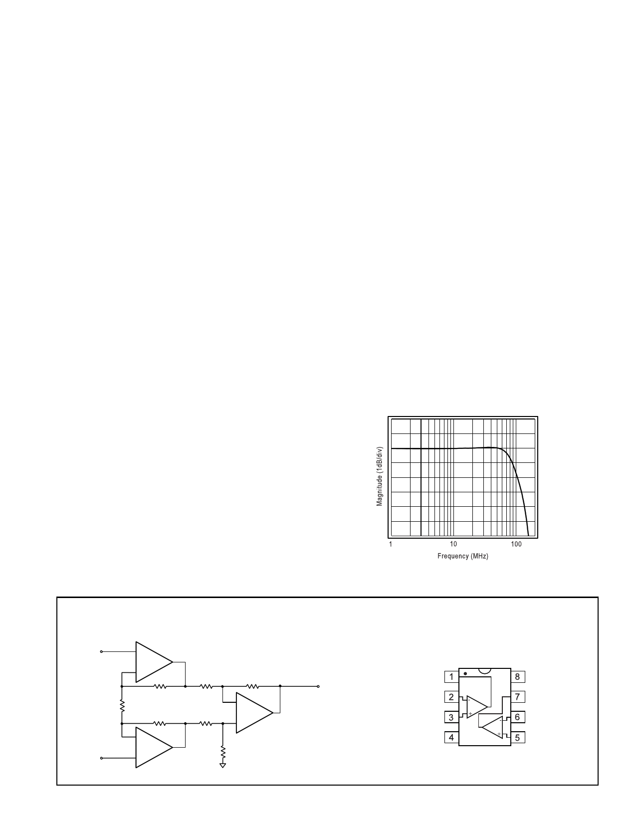
Frequency Response (Av = +2V/V)
V1
348Ω
V2
Typical Application Diagram
Instrumentation Amplifier
+
1/2
CLC416
-
348Ω
348Ω
-
1/2
CLC416
+
348Ω
348Ω
348Ω
-
CLC405
+
R1
348Ω
Vout = 3(V2 - V1)
© 1998 National Semiconductor Corporation
Printed in the U.S.A.
Pinout
DIP & SOIC
Vo1
Vinv1
Vnon-inv1
-VCC
+VCC
Vo2
Vinv2
Vnon-inv2
http://www.national.com
1 page 
-20
-40
-60
-80
-100
-120
1
10
Frequency (MHz)
100
Figure 3: Input Referred Crosstalk vs. Frequency
Driving Cables and Capacitive Loads
When driving cables, double termination is used to
prevent reflections. For capacitive load applications, a
small series resistor at the output of the CLC416 will
improve stability. The Rs vs. Capacitive Load plot,
in the Typical Performance section, gives the
recommended series resistance value for optimum
flatness at various capacitive loads.
Power Dissipation
The power dissipation of an amplifier can be described
in two conditions:
s Quiescent Power Dissipation -
PQ (No Load Condition)
s Total Power Dissipation -
PT (with Load Condition)
The following steps can be taken to determine the
power consumption for each CLC416 amplifier:
1. Determine the quiescent power
PQ = Icc (VCC - VEE)
2. Determine the RMS power at the output stage
PO = (Vcc - Vload) (Iload), where Vload and Iload
are the RMS voltage and current across the
external load.
3. Determine the total RMS power
PT = PQ + PO
Add the total RMS powers for both channels to deter-
mine the power dissipated by the dual.
evaluation boards for the CLC416 (CLC730038 - DIP,
CLC730036 - SOIC) and suggests their use as a guide
for high frequency layout and as an aid for device test-
ing and characterization.
Supply bypassing is required for best performance.
The bypass capacitors provide a low impedance return
current path at the supply pins. They also provide high
frequency filtering on the power supply traces. Other
layout factors play a major role in high frequency
performance. The following are recommended as a
basis for high frequency layout:
1. Include 6.8µF tantalum and 0.1µF ceramic
capacitors on both supplies.
2. Place the 6.8µF capacitors within 0.75 inches
of the power pins.
3. Place the 0.1µF capacitors within 0.1 inches
of the power pins.
4. Remove the ground plane under and around
the part, especially near the input and output
pins to reduce parasitic capacitance.
5. Minimize all trace lengths to reduce series
inductances.
Additional information is included in the evaluation
board literature.
SPICE Models
SPICE models provide a means to evaluate amplifier
designs. Free SPICE models are available for
National’s monolithic amplifiers that:
s Support Berkeley SPICE 2G and its many
derivatives
s Reproduce typical DC, AC, Transient, and
Noise performance
s Support room temperature simulations
The readme file that accompanies the diskette lists
released models, and provides a list of modeled para-
meters. The application note OA-18, Simulation
SPICE Models for National’s Op Amps, contains
schematics and a reproduction of the readme file.
Applications Circuits
The maximum power that the package can dissipate at
a given temperature is illustrated in the Power
Derating curves in the Typical Performance section.
The power derating curve for any package can be
derived by utilizing the following equation:
P=
(175° − Tamb)
θ JA
where: Tamb = Ambient temperature (°C)
θJA = Thermal resistance, from junction to
ambient, for a given package (°C/W)
Layout Considerations
A proper printed circuit layout is essential for achieving
high frequency performance. National provides
Instrumentation Amplifier
An instrumentation circuit is shown on the front page
and reproduced in Figure 4. The DC CMRR can be
fine tuned by adjusting R1.
V1 +
1/2
CLC416
-
348Ω
348Ω
V2
348Ω
-
1/2
CLC416
+
348Ω
348Ω
348Ω
-
CLC405
+
R1
348Ω
Vout = 3(V2 - V1)
Figure 4: Instrumentation Amplifier
5 http://www.national.com
5 Page | ||
| Páginas | Total 6 Páginas | |
| PDF Descargar | [ Datasheet CLC416AJ.PDF ] | |
Hoja de datos destacado
| Número de pieza | Descripción | Fabricantes |
| CLC416AJ | Dual Low-Power/ 120MHz Op Amp | National Semiconductor |
| Número de pieza | Descripción | Fabricantes |
| SLA6805M | High Voltage 3 phase Motor Driver IC. |
Sanken |
| SDC1742 | 12- and 14-Bit Hybrid Synchro / Resolver-to-Digital Converters. |
Analog Devices |
|
DataSheet.es es una pagina web que funciona como un repositorio de manuales o hoja de datos de muchos de los productos más populares, |
| DataSheet.es | 2020 | Privacy Policy | Contacto | Buscar |