|
|
|
PDF FM25V01 Data sheet ( Hoja de datos )
| Número de pieza | FM25V01 | |
| Descripción | 128Kb Serial 3V F-RAM Memory | |
| Fabricantes | Cypress Semiconductor | |
| Logotipo | ||
Hay una vista previa y un enlace de descarga de FM25V01 (archivo pdf) en la parte inferior de esta página. Total 18 Páginas | ||
|
No Preview Available !
FM25V01
128Kb Serial 3V F-RAM Memory
Features
128K bit Ferroelectric Nonvolatile RAM
Organized as 16,384 x 8 bits
High Endurance 100 Trillion (1014) Read/Writes
10 Year Data Retention
NoDelay™ Writes
Advanced High-Reliability Ferroelectric Process
Very Fast Serial Peripheral Interface - SPI
Up to 40 MHz Frequency
Direct Hardware Replacement for Serial Flash
SPI Mode 0 & 3 (CPOL, CPHA=0,0 & 1,1)
Write Protection Scheme
Hardware Protection
Software Protection
Description
The FM25V01 is a 128-kilobit nonvolatile memory
employing an advanced ferroelectric process. A
ferroelectric random access memory or F-RAM is
nonvolatile and performs reads and writes like a
RAM. It provides reliable data retention for 10 years
while eliminating the complexities, overhead, and
system level reliability problems caused by Serial
Flash and other nonvolatile memories.
Unlike Serial Flash, the FM25V01 performs write
operations at bus speed. No write delays are incurred.
Data is written to the memory array immediately
after it has been transferred to the device. The next
bus cycle may commence without the need for data
polling. The product offers very high write
endurance, orders of magnitude more endurance than
Serial Flash. Also, F-RAM exhibits lower power
consumption than Serial Flash.
These capabilities make the FM25V01 ideal for
nonvolatile memory applications requiring frequent
or rapid writes or low power operation. Examples
range from data collection, where the number of
write cycles may be critical, to demanding industrial
controls where the long write time of Serial Flash can
cause data loss.
The FM25V01 provides substantial benefits to users
of Serial Flash as a hardware drop-in replacement.
The device uses the high-speed SPI bus, which
Device ID
Device ID reads out Manufacturer ID & Part ID
Low Voltage, Low Power
Low Voltage Operation 2.0V – 3.6V
Active Current 120 A (typ. @ 1MHz)
Standby Current 90 A (typ.)
Sleep Mode Current 5 A (typ.)
Industry Standard Configurations
Industrial Temperature -40 C to +85 C
8-pin “Green”/RoHS SOIC Package
enhances the high-speed write capability of F-RAM
technology. The device incorporates a read-only
Device ID that allows the host to determine the
manufacturer, product density, and product revision.
The device is guaranteed over an industrial
temperature range of -40°C to +85°C.
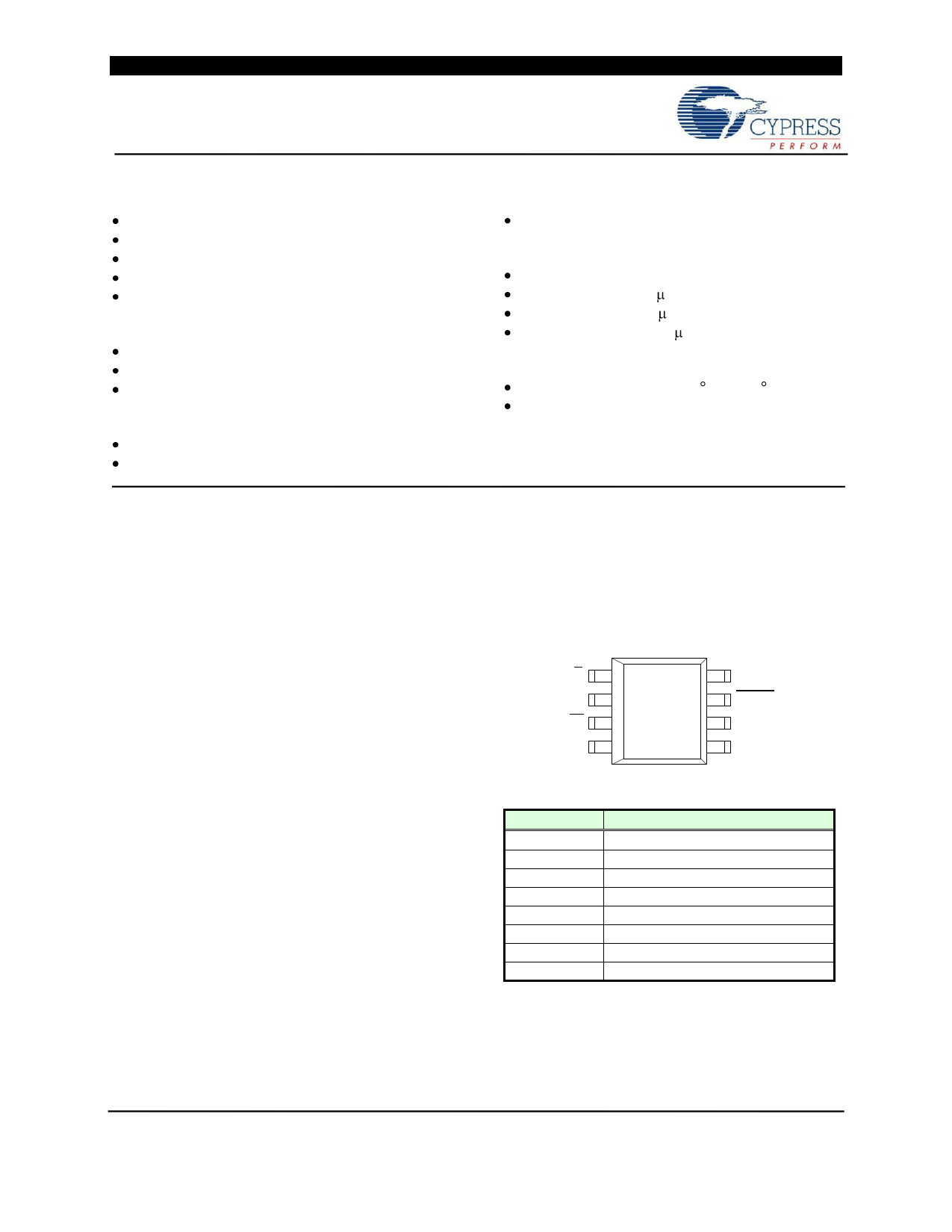
Pin Configuration
S
Q
W
VSS
1
2
3
4
8 VDD
7 HOLD
6C
5D
Pin Name
/S
/W
/HOLD
C
D
Q
VDD
VSS
Function
Chip Select
Write Protect
Hold
Serial Clock
Serial Data Input
Serial Data Output
Supply Voltage
Ground
This product conforms to specifications per the terms of the Ramtron standard warranty. The product has completed Ramtron’s
internal qualification testing and has reached production status.
Cypress Semiconductor Corporation • 198 Champion Court • San Jose, CA 95134-1709 • 408-943-2600
Document Number: 001-84492 Rev. *B
Revised May 29, 2013
1 page 
Power Up to First Access
The FM25V01 is not accessible for a period of time
(tPU) after power up. Users must comply with the
timing parameter tPU, which is the minimum time
from VDD (min) to the first /S low.
Data Transfer
All data transfers to and from the FM25V01 occur in
8-bit groups. They are synchronized to the clock
signal (C), and they transfer most significant bit
(MSB) first. Serial inputs are registered on the rising
edge of C. Outputs are driven from the falling edge of
clock C.
Command Structure
There are ten commands called op-codes that can be
issued by the bus master to the FM25V01. They are
listed in the table below. These op-codes control the
functions performed by the memory. They can be
divided into three categories. First, there are
commands that have no subsequent operations. They
perform a single function, such as to enable a write
operation. Second are commands followed by one
byte, either in or out. They operate on the Status
Register. The third group includes commands for
memory transactions followed by address and one or
more bytes of data.
Table 1. Op-code Commands
Name Description
WREN Set Write Enable Latch
WRDI Write Disable
RDSR Read Status Register
WRSR Write Status Register
READ Read Memory Data
FSTRD Fast Read Memory Data
WRITE Write Memory Data
SLEEP Enter Sleep Mode
RDID Read Device ID
Op-code
0000 0110b
0000 0100b
0000 0101b
0000 0001b
0000 0011b
0000 1011b
0000 0010b
1011 1001b
1001 1111b
WREN – Set Write Enable Latch
The FM25V01 will power up with writes disabled.
The WREN command must be issued prior to any
write operation. Sending the WREN op-code will
allow the user to issue subsequent op-codes for write
operations. These include writing the Status Register
(WRSR) and writing the memory (WRITE).
Sending the WREN op-code causes the internal Write
Enable Latch to be set. A flag bit in the Status
Register, called WEL, indicates the state of the latch.
WEL=1 indicates that writes are permitted.
Attempting to write the WEL bit in the Status
Register has no effect on the state of this bit.
Completing any write operation will automatically
clear the write-enable latch and prevent further writes
Document Number: 001-84492 Rev. *B
FM25V01 - 128Kb SPI FRAM
without another WREN command. Figure 5 below
illustrates the WREN command bus configuration.
S
01234567
C
D 00000110
Q Hi-Z
Figure 5. WREN Timing
WRDI – Write Disable
The WRDI command disables all write activity by
clearing the Write Enable Latch. The user can verify
that writes are disabled by reading the WEL bit in
the Status Register and verifying that WEL=0.
Figure 6 illustrates the WRDI command bus
configuration.
S
01234567
C
D 00000100
Q Hi-Z
Figure 6. WRDI Timing
RDSR – Read Status Register
The RDSR command allows the bus master to
verify the contents of the Status Register. Reading
Status provides information about the current state
of the write protection features. Following the
RDSR op-code, the FM25V01 will return one byte
with the contents of the Status Register. The Status
Register is described in detail in the section below.
Page 5 of 18
5 Page 
FM25V01 - 128Kb SPI FRAM
Electrical Specifications
Absolute Maximum Ratings
Symbol
Description
VDD Power Supply Voltage with respect to VSS
VIN Voltage on any pin with respect to VSS
TSTG
TLEAD
VESD
Storage Temperature
Lead Temperature (Soldering, 10 seconds)
Electrostatic Discharge Voltage
- Human Body Model (AEC-Q100-002 Rev. E)
- Charged Device Model (AEC-Q100-011 Rev. B)
- Machine Model (AEC-Q100-003 Rev. E)
Package Moisture Sensitivity Level
Ratings
-1.0V to +4.5V
-1.0V to +4.5V
and VIN < VDD+1.0V
-55 C to + 125 C
260 C
TBD
1.25kV
200V
MSL-1
Stresses above those listed under Absolute Maximum Ratings may cause permanent damage to the device. This is a stress rating
only, and the functional operation of the device at these or any other conditions above those listed in the operational section of this
specification is not implied. Exposure to absolute maximum ratings conditions for extended periods may affect device reliability.
DC Operating Conditions (TA = -40 C to + 85 C, VDD = 2.0V to 3.6V unless otherwise specified)
Symbol Parameter
Min Typ
Max Units Notes
VDD Power Supply Voltage
IDD Power Supply Operating Current
@ C = 1 MHz
2.0 3.3
3.6
V
1
0.12 0.22 mA
@ C = 40 MHz
1.3 2.5 mA
ISB Standby Current
IZZ Sleep Mode Current
ILI Input Leakage Current
ILO Output Leakage Current
90 150
A2
58
A3
- 1 A4
- 1 A4
VIH
VIL
VOH1
VOH2
VOL1
VOL2
RIN
Input High Voltage
Input Low Voltage
Output High Voltage (IOH = -1 mA, VDD=2.7V)
Output High Voltage (IOH = -100 A)
Output Low Voltage (IOL = 2 mA, VDD=2.7V)
Output Low Voltage (IOL = 150 A)
Input Resistance (/HOLD pin)
For VIN = VIH (min)
For VIN = VIL (max)
0.7 VDD
-0.3
2.4
VDD-0.2
-
-
40
1
VDD + 0.3
0.3 VDD
-
-
0.4
0.2
V
V
V
V
V
V
K
M
5
Notes
1. C toggling between VDD-0.2V and VSS, other inputs VSS or VDD-0.2V.
2. /S=VDD. All inputs VSS or VDD.
3. In Sleep mode and /S=VDD. All inputs VSS or VDD.
4. VSS VIN VDD and VSS VOUT VDD.
5. The input pull-up circuit is stronger (> 40K ) when the input voltage is above VIH and weak (> 1M ) when the input
voltage is below VIL.
Data Retention (TA = -40 C to + 85 C)
Parameter
Data Retention
Min
Max
Units
Notes
10 - Years
Document Number: 001-84492 Rev. *B
Page 11 of 18
11 Page | ||
| Páginas | Total 18 Páginas | |
| PDF Descargar | [ Datasheet FM25V01.PDF ] | |
Hoja de datos destacado
| Número de pieza | Descripción | Fabricantes |
| FM25V01 | 128Kb Serial 3V F-RAM Memory | Cypress Semiconductor |
| FM25V01 | 3V F-RAM Memory | Ramtron |
| FM25V01A | 128-Kbit (16K x 8) Serial (SPI) F-RAM | Cypress Semiconductor |
| FM25V02 | 3V F-RAM Memory | Ramtron |
| Número de pieza | Descripción | Fabricantes |
| SLA6805M | High Voltage 3 phase Motor Driver IC. |
Sanken |
| SDC1742 | 12- and 14-Bit Hybrid Synchro / Resolver-to-Digital Converters. |
Analog Devices |
|
DataSheet.es es una pagina web que funciona como un repositorio de manuales o hoja de datos de muchos de los productos más populares, |
| DataSheet.es | 2020 | Privacy Policy | Contacto | Buscar |