|
|
|
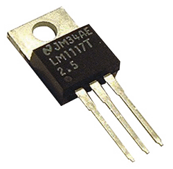
PDF LM1117 Data sheet ( Hoja de datos )
| Número de pieza | LM1117 | |
| Descripción | 1A L.D.O VOLTAGE REGULATOR | |
| Fabricantes | HTC | |
| Logotipo | ||
 1. Datasheet - 800mA Linear Regulator Hay una vista previa y un enlace de descarga de LM1117 (archivo pdf) en la parte inferior de esta página. Total 12 Páginas | ||
|
No Preview Available !
1A L.D.O VOLTAGE REGULATOR
FEATURES
z Output Current up to 1 A
z Low Dropout Voltage (1.2V at 1A Output current)
z Three Terminal Adjustable(ADJ) or Fixed 1.2V, 1.5V,
1.8V, 2.5V, 2.85V, 3.3V, 5.0V
z Line Regulation typically at 0.1% max.
z Load Regulation typically at 0.2% max.
z Internal Current and Terminal Protection
z Maximum Input Voltage 20V
z Surface Mount Package SOT-223, TO-252, SOT-89
z 100% Thermal Limit Burn-In
z Moisture Sensitivity Level 3
LM1117
SOT-223 PKG
TO-252 PKG
SOT-89 PKG
APPLICATION
z Active SCSI Terminators
z Portable/ Plan Top/ Notebook Computers
z High Efficiency Linear Regulators
z SMPS Post Regulators
z Mother B/D Clock Supplies
z Disk Drives
z Battery Chargers
DESCRIPSION
ORDERING INFORMATION
Device
Package
LM1117S-ADJ
LM1117S-X.X
LM1117GS-ADJ
SOT-223 3L
LM1117GS-X.X
LM1117RS-ADJ
LM1117RS-X.X
LM1117GRS-ADJ
TO-252 3L
LM1117GRS-X.X
LM1117F-ADJ
LM1117F-X.X
LM1117GF-ADJ
SOT-89 3L
LM1117GF-X.X
X.X = Output Voltage = 1.2V, 1.5V, 1.8V, 2.5V, 2.85V,
3.3V, 5.0V
The LM1117 is a low power positive-voltage regulator designed to meet 1A output current and comply with SCSI-II
specifications with a fixed output voltage of 2.85V. This device is an excellent choice for use in battery-powered
applications, as active terminators for the SCSI bus, and portable computers. The LM1117 features very low
quiescent current and very low dropout voltage of 1V at a full load and lower as output current decreases.
LM1117 is available as an adjustable or fixed 1.2V, 1.5V, 1.8V, 2.5V, 2.85, 3.3V, and 5.0V output voltages. The
LM1117 is offered in a 3-pin surface mount package SOT-223, TO-252 & SOT-89. The output capacitor of 10㎌ or
larger is needed for output stability of LM1117 as required by most of the other regulator circuits.
Absolute Maximum Ratings
(TA = 25℃, unless otherwise specified)
CHARACTERISTIC
DC Input Voltage
Lead Temperature (Soldering, 5 seconds)
Operating Junction Temperature Range
Storage Temperature Range
Mar. 2013 Rev. 1.22
SYMBOL
VIN
TSOL
TOPR
TSTG
-1-
MIN.
-
-
-40
-65
MAX.
20
260
125
150
UNIT
V
℃
℃
℃
HTC
1 page 
1A L.D.O VOLTAGE REGULATOR
LM1117
ELECTRICAL CHARACTERISTICS
For ADJ Output Voltage
Symbol
Parameters
Condition
(TA=25℃, CO = 10uF unless otherwise specified)
Min. Typ. Max. Unit
VREF
Reference Voltage
VREF
Reference Voltage
ΔVLINE Line Regulation
VIN=5V, IO=10mA
IO = 10mA to 1A, VIN - VREF = 1.5V to
13.75V (TJ = 0 ~ 125℃)
IO = 10mA , VIN - VREF = 1.5V to 12V
1.238
1.219
1.250
0.1
1.262
1.281
0.2
V
V
%
ΔVLOAD Load Regulation
IO = 10mA to 1A, VIN - VREF = 2 V
0.2 0.4
%
VIN Operating Input Voltage
12 V
IADJ
ΔIADJ
IO(MIN)
Adjustment pin Current VIN - VREF = 1.5V to 12V, IO = 100mA
Adjustment Pin Current VIN - VREF = 1.5V to 12V,
Change
IO = 100mA to 1A
Minimum Load Current
VIN=5V, VREF=0V
50 120 uA
0.5 5 uA
5 10 mA
IO Current Limit
VIN - VREF = 5V
1000
1250
1600
mA
EN
SVR
Output Noise(%VO)
Supply Voltage Rejection
B = 10Hz to 10kHz, TJ = 25℃
IO = 1A, f = 120Hz,
VIN - VREF = 3V, VRIPPLE = 1VPP
0.003
60 75
%
dB
For 1.2V Output Voltage
Symbol
Parameters
Condition
(TA=25℃, CO = 10uF unless otherwise specified)
Min. Typ. Max. Unit
VO Output Voltage
VO Output Voltage
ΔVLINE Line Regulation
VIN = 2.7V, IO = 10mA
VIN = 2.7V to 12V, IO = 0mA to 1A
(TJ = 0 ~ 125℃)
IO = 0mA , VIN = 2.7V to 12V
1.176
1.152
1.200
0.1
1.224
1.248
0.2
V
V
%
ΔVLOAD Load Regulation
IO = 10mA to 1A, VIN = 3.2V
0.2 0.4
%
VIN Operating Input Voltage
12 V
ID Quiescent Current
VIN - VO = 5V
5 10 ㎃
IO Current Limit
VIN - VO = 5V
1000
1250
1600
㎃
EN
SVR
Output Noise(%VO)
Supply Voltage Rejection
B = 10Hz to 10kHz, TJ = 25℃
IO = 1A, f = 120Hz,
VIN - VO = 1.5V, VRIPPLE = 1VPP
0.003
60 75
%
dB
Mar. 2013 Rev. 1.22
-5-
HTC
5 Page 
1A L.D.O VOLTAGE REGULATOR
TYPICAL OPERATING CHARACTERISTICS
LM1117
Fig.7 OUTPUT VOLTAGE CHANGE VS TEMPERATURE
Fig.8 DROPOUT VOLTAGE VS OUTPUT CURRENT
Fig.9 OUTPUT SHORT CIRCUIT CURRENT VS
DIFFERENTIAL VOLTAGE
Fig.10 OUTPUT SHORT CIRCUIT CURRENT VS
TEMPERATURE
Fig.11 ADJ PIN CURRENT VS TEMPERATURE
Fig.12 QUIESCENT CURRENT CHANGE VS TEMPERATURE
Mar. 2013 Rev. 1.22
- 11 -
HTC
11 Page | ||

| Páginas | Total 12 Páginas | |
| PDF Descargar | [ Datasheet LM1117.PDF ] | |
Hoja de datos destacado
| Número de pieza | Descripción | Fabricantes |
| LM111 | Voltage Comparator | National Semiconductor |
| LM111 | Voltage comparator | NXP Semiconductors |
| LM111 | VOLTAGE COMPARATORS | STMicroelectronics |
| LM111 | Voltage comparator | NXP Semiconductors |
| Número de pieza | Descripción | Fabricantes |
| SLA6805M | High Voltage 3 phase Motor Driver IC. |
Sanken |
| SDC1742 | 12- and 14-Bit Hybrid Synchro / Resolver-to-Digital Converters. |
Analog Devices |
|
DataSheet.es es una pagina web que funciona como un repositorio de manuales o hoja de datos de muchos de los productos más populares, |
| DataSheet.es | 2020 | Privacy Policy | Contacto | Buscar |