|
|
|
PDF PI4ULS3V502 Data sheet ( Hoja de datos )
| Número de pieza | PI4ULS3V502 | |
| Descripción | 280Mb/s Bi-directional Level Translator | |
| Fabricantes | Pericom Semiconductor | |
| Logotipo | ||
Hay una vista previa y un enlace de descarga de PI4ULS3V502 (archivo pdf) en la parte inferior de esta página. Total 9 Páginas | ||
|
No Preview Available !
PI4ULS3V502
|||||||||||||||||||||||||||||||||||||||||||||||||||||||||||||||||||||||||||||||||||||||||||||||||||||||||||||||||||||||||||||||||||||||||||||||||||||||||||||||||||||||||||||||||||||||||||||||||||||||||||||||||||||||||||||||||||||||||||||||||||||||||||||||||||||||||||||||||||||||||||||||||||||||||||||||||||||||||||||||||||||||
280Mb/s Bi-directional Level Translator for Push-Pull Applications
Features
0.85V to 2.7V on A Port and 1.35V to 3.6V on B
Port
VCCA may be greater than, equal to, or less than
VCCB
High-Speed with 280 Mb/s Guaranteed Date Rate
30 pF Capacitive Drive Capability
Low Bit-to-Bit Skew
Overvoltage Tolerant Enable and I/O Pins
Non-preferential Power-Up Sequencing
Power-Off Protection
Package: UDFN1.2x1.6-8L
Applications
Mobile Phones, PDAs
Other Portable Devices
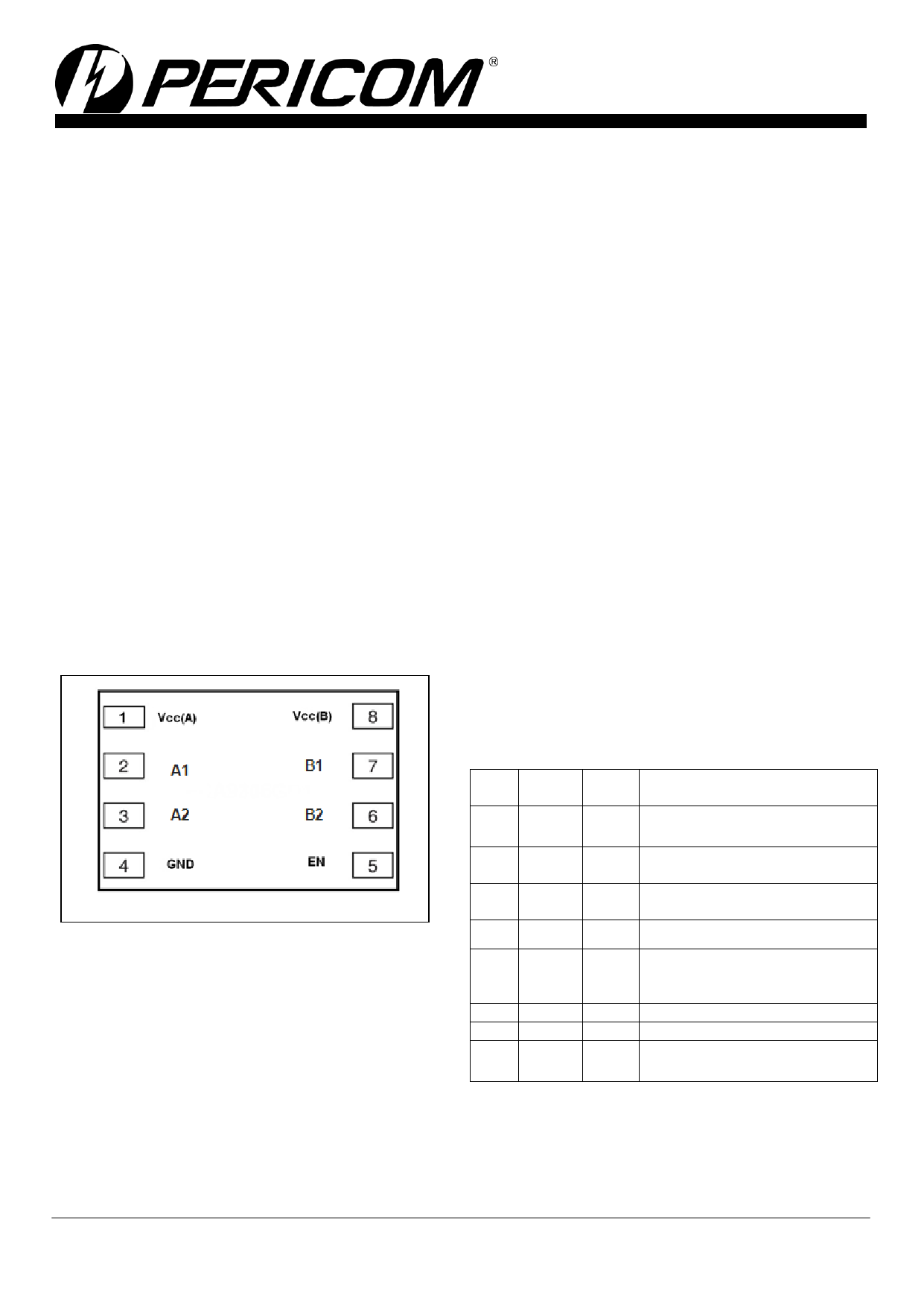
Pin Configuration
Description
The PI4ULS3V502 is a 2-bit configurable dual-
supply autosensing bidirectional level translator that
does not require a direction control pin. The B and A
ports are designed to track two different power supply
rails, VCCB and VCCA respectively.
The PI4ULS3V502 offers the feature that the values
of the VCCB and VCCA supplies are independent.
Design flexibility is maximized because VCCA can be
set to a value either greater than or less than the VCCB
supply.
The PI4ULS3V502 has high output current
capability, which allows the translator to drive high
capacitive loads such as most high frequency EMI filters.
Another feature of the PI4ULS3V502 is that each An
and Bn channel can function as either an input or an
output.
An Output Enable (EN) input is available to reduce
the power consumption. The EN pin can be used to
disable both I/O ports by putting them in 3-state which
significantly reduces the supply current.
PI4ULS3V502 is 2 kV System-Level ESD Capable.
Pin Description
UDFN1.2*1.6-8L(Top View)
Pin Pin Type
Description
No. Name
1
VCCA
Power
A-port supply voltage.0.85V ≤
VCCA ≤ 2.7V
2
A1
I/O
Input/output A. Referenced to
VCCA.
3
A2
I/O
Input/output A. Referenced to
VCCA.
4 GND GND Ground.
Output enable (active High). Pull
5 EN Input EN low to place all outputs in 3-
state mode.
6 B2 I/O Input/output B. Referenced to VCCB
7 B1 I/O Input/output B. Referenced to VCCB
8
VCCB
Power
B-port supply voltage. 1.35 V ≤
VCCB ≤ 3.6V
2014-01-0006
PT0475-1 02/18/14
1
1 page 
PI4ULS3V502
280Mb/s Bi-directional Level Translator
for Push-Pull Applications
|||||||||||||||||||||||||||||||||||||||||||||||||||||||||||||||||||||||||||||||||||||||||||||||||||||||||||||||||||||||||||||||||||||||||||||||||||||||||||||||||||||||||||||||||||||||||||||||||||||||||||||||||||||||||||||||||||||||||||||||||||||||||||||||||||||||||||||||||||||||||||||||||||||||||||||||||||||||||||||||||||||||
4. Typical values are for B = +2.8 V, A = +1.8 V and TA = +25°C. All units are production tested at TA = +25°C. Limits over the
operating temperature range are guaranteed by design.
5. Guaranteed by design.
Power Consumption (TA =25°C)
Symbol*1 Parameter
Test Conditions
CPD_VCCA
A = Input port,
B = Output
Port
B = Input port,
A = Output
Port
CLoad = 0, f = 1MHz,
EN = VCCA (outputs enabled)
CLoad = 0, f = 1MHz,
EN = VCCA (outputs enabled)
VCCB (V)*2 VCCA (V)*3
1.35 - 3.6 0.85 - 2.7
Typ*4
40
Unit
pF
1.35 - 3.6 0.85 - 2.7 40 pF
CPD_VCCB
A = Input port,
B = Output
Port
B = Input port,
A = Output
Port
CLoad = 0, f = 1MHz,
EN = VCCA (outputs enabled)
CLoad = 0, f = 1MHz,
EN = VCCA (outputs enabled)
1.35 - 3.6 0.85 - 2.7
1.35 - 3.6 0.85 - 2.7
40 pF
40 pF
A = Input port,
B = Output
Port
CLoad = 0, f = 1MHz,
EN = GND (outputs disabled)
1.35 - 3.6 0.85 - 2.7
1
pF
CPD_VCCA B = Input port,
A = Output
Port
CLoad = 0, f = 1MHz,
EN = GND (outputs disabled)
1.35 - 3.6 0.85 - 2.7
1
pF
CPD_VCCB
A = Input port,
B = Output
Port
B = Input port,
A = Output
Port
CLoad = 0, f = 1MHz,
EN = GND (outputs disabled)
CLoad = 0, f = 1MHz,
EN = GND (outputs disabled)
1.35 - 3.6 0.85 - 2.7
1.35 - 3.6 0.85 - 2.7
1
1
pF
pF
Notes:
1. CPD_VCCA and CPD_VCCB are defined as the value of the IC’s equivalent capacitance from which the operating current can be
calculated for the A and B power supplies, respectively. ICC = ICC (dynamic) + ICC (static) ≈ICC(operating) ≈CPD x VCC x fIN x
NSW where ICC = ICC_VCCB+ ICC_VCCA and NSW = total number of outputs switching.
2. VCCB is the supply voltage associated with the I/O B port, and VCCB ranges from +1.35V to 3.6V under normal operating
conditions.
3. VCCA is the supply voltage associated with the I/O A port, and VCCA ranges from +0.8 V to 2.7V under normal operating
conditions.
4. Typical values are at TA = +25°C.
2014-01-0006
PT0475-1 02/18/14
5
5 Page | ||
| Páginas | Total 9 Páginas | |
| PDF Descargar | [ Datasheet PI4ULS3V502.PDF ] | |
Hoja de datos destacado
| Número de pieza | Descripción | Fabricantes |
| PI4ULS3V501 | 280Mb/s Bi-directional Level Translator | Pericom Semiconductor |
| PI4ULS3V502 | 280Mb/s Bi-directional Level Translator | Pericom Semiconductor |
| PI4ULS3V504 | 280Mb/s Bi-directional Level Translator | Pericom Semiconductor |
| Número de pieza | Descripción | Fabricantes |
| SLA6805M | High Voltage 3 phase Motor Driver IC. |
Sanken |
| SDC1742 | 12- and 14-Bit Hybrid Synchro / Resolver-to-Digital Converters. |
Analog Devices |
|
DataSheet.es es una pagina web que funciona como un repositorio de manuales o hoja de datos de muchos de los productos más populares, |
| DataSheet.es | 2020 | Privacy Policy | Contacto | Buscar |