|
|
|
PDF R7779 Data sheet ( Hoja de datos )
| Número de pieza | R7779 | |
| Descripción | Burst Triple-Mode PWM Controller | |
| Fabricantes | RICHPOWER | |
| Logotipo | ||
Hay una vista previa y un enlace de descarga de R7779 (archivo pdf) en la parte inferior de esta página. Total 13 Páginas | ||
|
No Preview Available !
R7779
Burst Triple-Mode PWM Controller with Integrated HV
Start-up Device for Zero Power Monitor Application
General Description
Features
The R7779 is a high-performance current mode PWM
controller with integrated HV start-up device inside. During
start-up, a current source through integrated HV device to
charge VDD capacitor for quick start-up while it dissipates
no loss in normal operation.
The R7779 provides the users a superior AC/DC power
application of higher efficiency, low external component
counts, and low cost solution. It features frequency jitter,
Under Voltage LockOut (UVLO), Leading Edge Blanking
(LEB), internal slope compensation in the tiny SOP-8
package. It offers complete protection coverage with Over
Temperature Protection (OTP), Over Load Protection
(OLP) and Over Voltage Protection (OVP).
Moreover, it also provides a special interface for zero power
application when the converter is in sleeping mode. EN/
DIS pin receives ON/OFF signal from secondary scalar
controller. During turning off, the controller will be shutdown
completely with pretty low power consumption.
Integrated HV Start-up Device
UVLO : 9V/16.5V
Current Mode Control
Built-in 65kHz Operation Frequency
Jittering Frequency
Internal PWM Leading Edge Blanking
Internal Slope Compensation
Compensated Burst Triple-Mode PWM
Cycle-by-Cycle Current Limit
Internal Auto Recovery OVP
Internal Auto Recovery OLP
Internal Auto Recovery OTP
Secondary Rectifier Short Protection
Soft Driving for Reducing EMI Noise
High Noise Immunity
RoHS Compliant and Halogen Free
Applications
Switching AC/DC Adaptor and Battery Charger
TV and Monitor Application
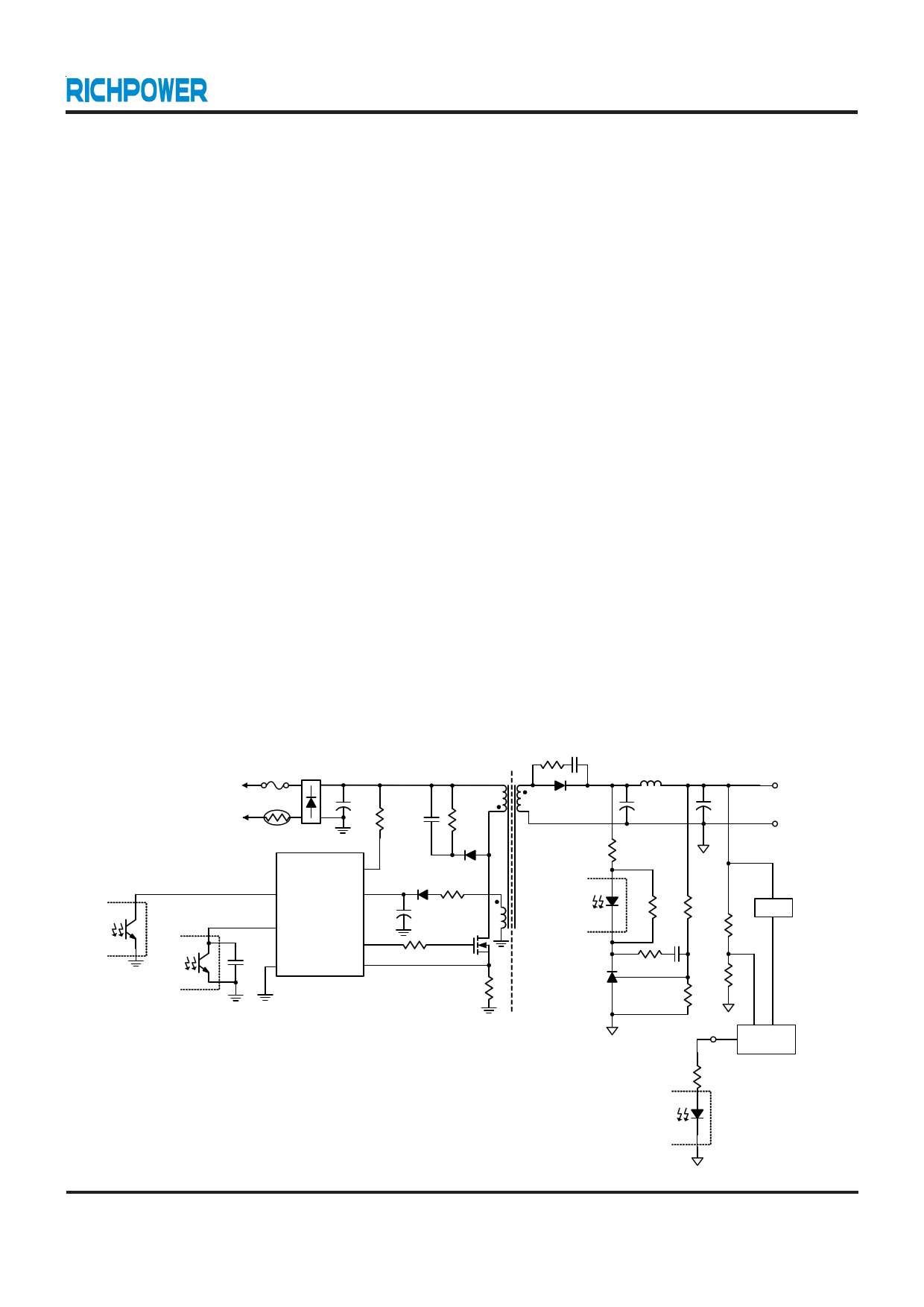
Typical Application Circuit
AC Mains
(90V to 265V)
OPTO2
OPTO1
R7779 HV
EN/DIS VDD
COMP
GND
GATE
CS
#
OPTO1
# See Application Information
VO+
VO-
# LDO
GPIO
Scalar
OPTO2
R7779-04 July 2009
1
1 page 
R7779
Parameter
Oscillator Section
Normal PWM Frequency
Maximum Duty Cycle
PWM Frequency Jitter Range
PWM Frequency Jitter Period
Frequency Variation Versus
VDD Deviation
Frequency Variation Versus
Temp. Deviation
COMP Input Section
Open Loop Voltage
Symbol
Conditions
fOSC
DCYMAX
△f
TJIT
fDV
For 65kHz
VDD = 12V to 25V
fDT TA = -30°C to 105°C
VCOMP_OP COMP pin open
COMP Open 56ms Protection
COMP Open-loop Protection Delay
Time
Short Circuit COMP Current
Current-Sense Section
VCOMP_56
TOLP
IZERO
VCOMP = 0V
Initial Current Limit Offset
Leading Edge Blanking Time
Internal Propagation Delay Time
Minimum On Time
GATE Section
VCSTH
TLEB
TPD
T ON _MIN
(Note 5)
(Note 5)
Gate Output Clamping Voltage
Rising Time
Falling Time
EN/DIS Interface Section
VCL AMP
TR
TF
VDD = 25V
VDD = 15V, CL = 1nF
VDD = 15V, CL = 1nF
Enable Threshold
VEN_TH
EN/DIS Pin Max Clamping Current
Min Typ Max Unit
60 65 70 kHz
70 75 80 %
-- ±7 -- %
-- 4 -- ms
-- -- 2 %
-- -- 5 %
5.5 5.75
5.25 --
6
--
-- 56 --
-- 1.3 2.5
V
V
ms
mA
0.72 0.75 0.78
150 250 350
-- 100 --
250 350 450
V
ns
ns
ns
-- 14 --
-- 125 --
-- 45 --
V
ns
ns
0.8 1 1.2 V
-- -- 30 µA
Note 1. Stresses beyond those listed under “ Absolute Maximum Ratings” may cause permanent damage to the device.
These are stress ratings only, and functional operation of the device at these or any other conditions beyond those
indicated in the operational sections of the specifications is not implied. Exposure to absolute maximum rating
conditions for extended periods may affect device reliability.
Note 2. θJA is measured in the natural convection at TA = 25°C on a low effective single layer thermal conductivity test board of
JEDEC 51-3 thermal measurement standard.
Note 3. Devices are ESD sensitive. Handling precaution is recommended.
Note 4. The device is not guaranteed to function outside its operating conditions.
Note 5. Leading edge blanking time and internal propagation delay time are guaranteed by design.
R7779-04 July 2009
5
5 Page 
after couples of cycle. It could pass CS pin open test
easier.
Secondary Rectifier Short Protection : As shown in
Figure 2. The current spike during secondary rectifier
short test is extremely high because of the saturated
main transformer. Meanwhile, the transformer acts like
a leakage inductance. During high line, the current in
power FET is sometimes too high to wait for a 56ms
OLP delay time. To offer better and easier protection
design, the R7779 shuts down the controller after
couples of cycles before fuse is blown up.
Secondary Rectifier Short
VDD
VCOMP
VCS
Figure 2. Secondary Rectifier Short Protection
R7779
R7779-04 July 2009
11
11 Page | ||
| Páginas | Total 13 Páginas | |
| PDF Descargar | [ Datasheet R7779.PDF ] | |
Hoja de datos destacado
| Número de pieza | Descripción | Fabricantes |
| R7779 | Burst Triple-Mode PWM Controller | RICHPOWER |
| Número de pieza | Descripción | Fabricantes |
| SLA6805M | High Voltage 3 phase Motor Driver IC. |
Sanken |
| SDC1742 | 12- and 14-Bit Hybrid Synchro / Resolver-to-Digital Converters. |
Analog Devices |
|
DataSheet.es es una pagina web que funciona como un repositorio de manuales o hoja de datos de muchos de los productos más populares, |
| DataSheet.es | 2020 | Privacy Policy | Contacto | Buscar |